





Content last revised on September 22, 2026
VS-85HFR40 Operational Boundaries: Evaluating Surge Energy Dissipation and Clamping Volt Limits
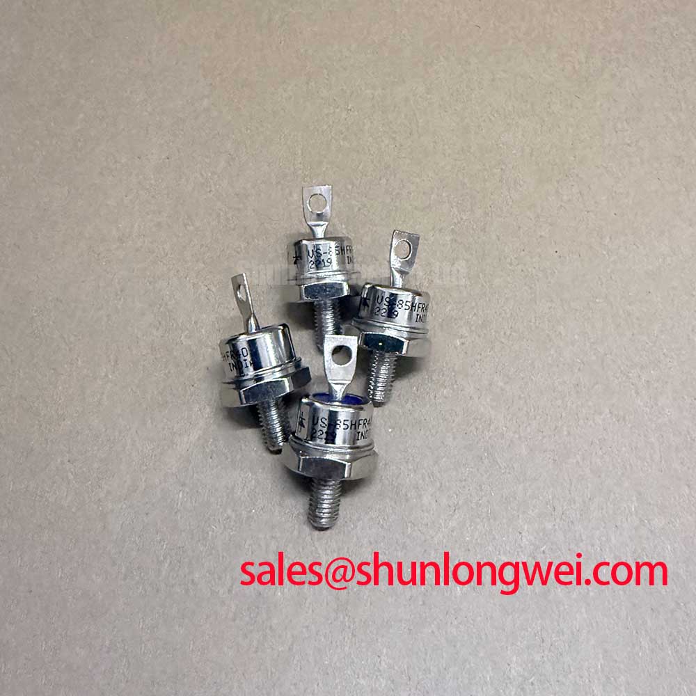
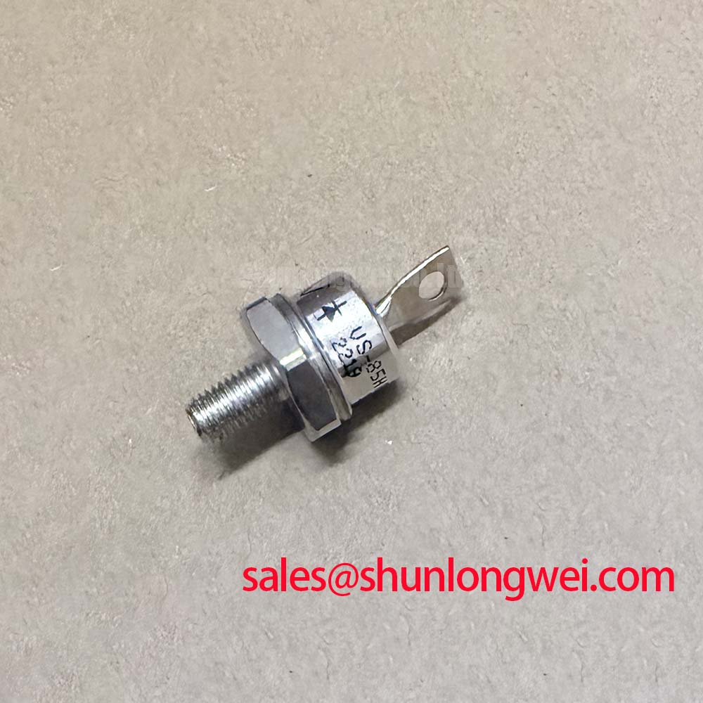
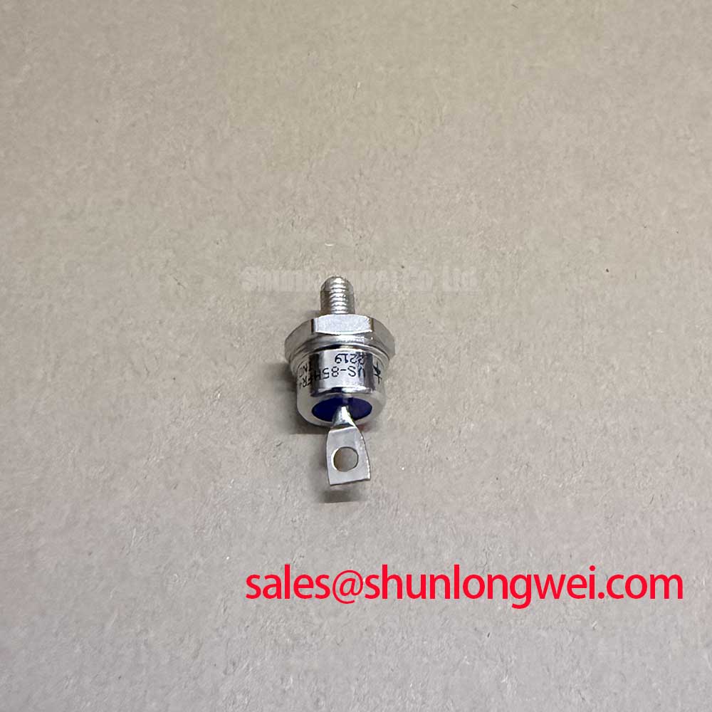
The Vishay VS-85HFR40 is a stud-mounted power semiconductor specified with a 400 V repetitive peak reverse voltage. Its stated average forward current is 85 A at a case temperature of 140 °C, while the maximum forward voltage is 1.2 V at 267 A and a junction temperature of 25 °C. These are official device specifications and should be kept separate from the surge capability, fuse coordination, and transient limits of the complete power converter.
For a medium-frequency induction melting or metal hardening power supply, the incoming protection network should be reviewed at the equipment level. An MOV placed ahead of the rectifier or controlled switching stage can help limit externally applied transient energy, but its voltage class, energy rating, and repeated surge capability must be selected from the actual line voltage, fault level, and coordination study. The 400 V reverse voltage rating of the device is not an MOV selection value and should not be treated as a permissible clamping target.
RC snubber placement is also system dependent. The network should be connected according to the converter topology and measured commutation behavior, with the resistor and capacitor selected after reviewing peak voltage, pulse energy, repetition rate, and damping requirements. Designers should verify the resulting semiconductor voltage margin during switching tests rather than infer it from the nominal VRRM rating alone.
Fuse coordination requires the manufacturer’s applicable surge current and I²t data for the exact circuit arrangement. The supplied factory parameter set does not include an I²t value or an ITSM rating, so those figures should be confirmed in the relevant Vishay documentation before specifying a semiconductor fuse. A fuse that protects wiring may not provide the required junction protection, and a fuse with an unsuitable clearing characteristic can expose the device to excessive thermal stress.
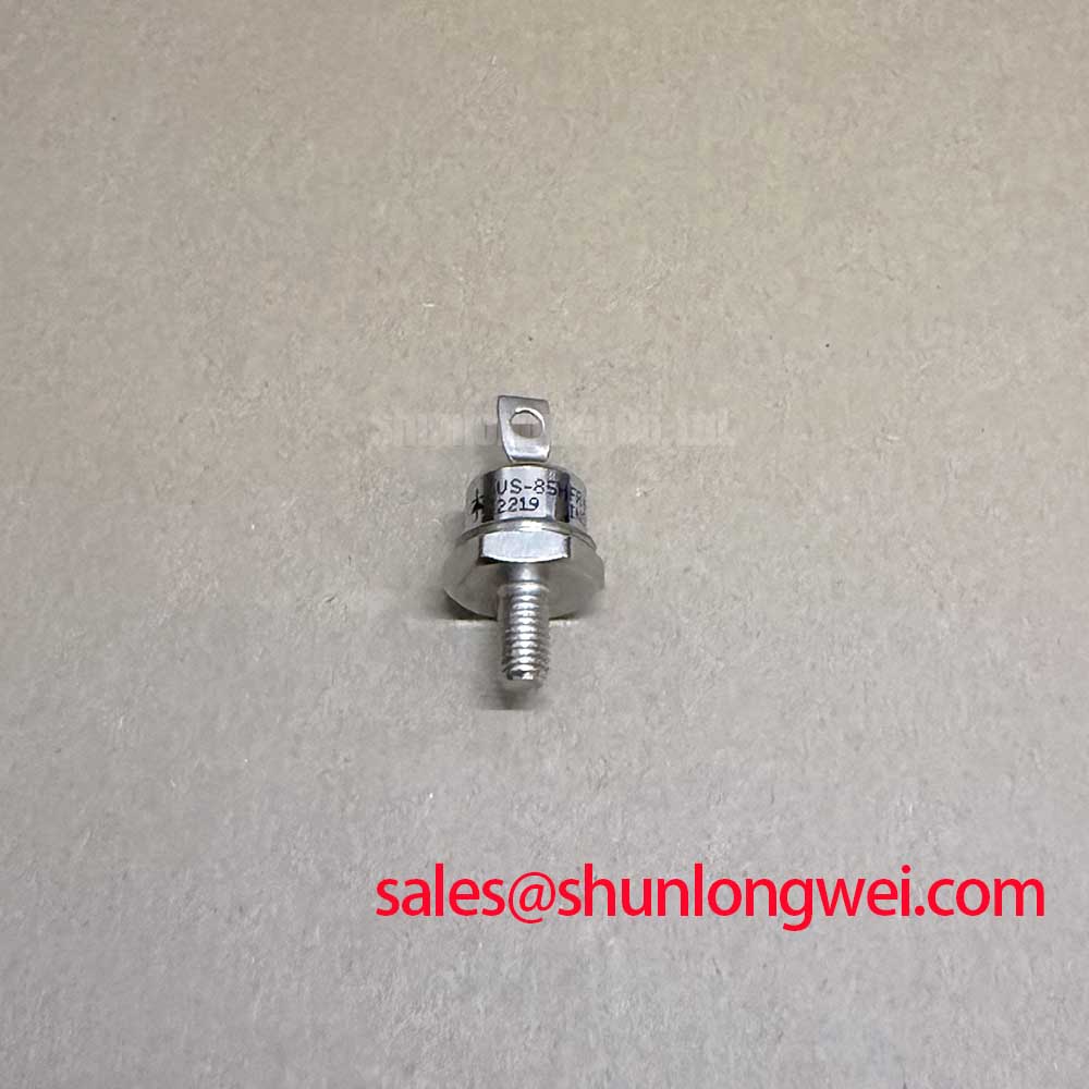
Terminal hardware must match the DO-203AB or DO-5 stud construction and the mating busbar or cable arrangement. Confirm thread form, washer arrangement, electrical contact area, insulation clearance, and mechanical torque from the original assembly documentation. Do not use a generic torque value as an official specification for this device. Creepage and clearance should be reviewed at the installed working voltage, pollution environment, and enclosure altitude.
Field Diagnostics & Commissioning: High-Frequency Switching Loss Dissipation in VS-85HFR40 Topologies
The listed specifications identify the forward-current capability and forward-voltage limit, but they do not provide reverse-recovery time, reverse-recovery charge, peak reverse-recovery current, or soft-recovery classification. Those characteristics are important when this device operates in a high-frequency commutation path. They must be taken from the applicable datasheet or validated on the assembled circuit rather than estimated from the 1.2 V forward-voltage figure.
During commissioning, inspect the current waveform at the semiconductor terminal and compare it with the voltage waveform across the device. An unexpected recovery spike, ringing, or elevated switching temperature may involve layout inductance, transformer leakage, snubber damping, timing in the surrounding circuit, or interaction with another rectifier path. Oscilloscope measurements should use a suitable differential voltage probe and a current measurement method appropriate for the switching frequency.
The VS-85HFR40 should not be assigned a specific switching-frequency limit from the five supplied factory parameters. A medium-frequency induction heating supply may impose substantially different commutation stress from a line-frequency rectifier. The system integrator should verify the actual junction temperature, peak repetitive voltage, current waveform, and transient behavior under the highest intended load and the most demanding line condition.
Where the unit is used in a rectification or auxiliary power stage, the surrounding circuit must be checked for correct terminal identification and polarity before power is applied. The available product information supplied here does not define a gate or trigger connection for this diode. Device-specific reverse-recovery and other dynamic parameters should be confirmed from the applicable documentation if the application uses controlled commutation or triggering in the surrounding circuit.
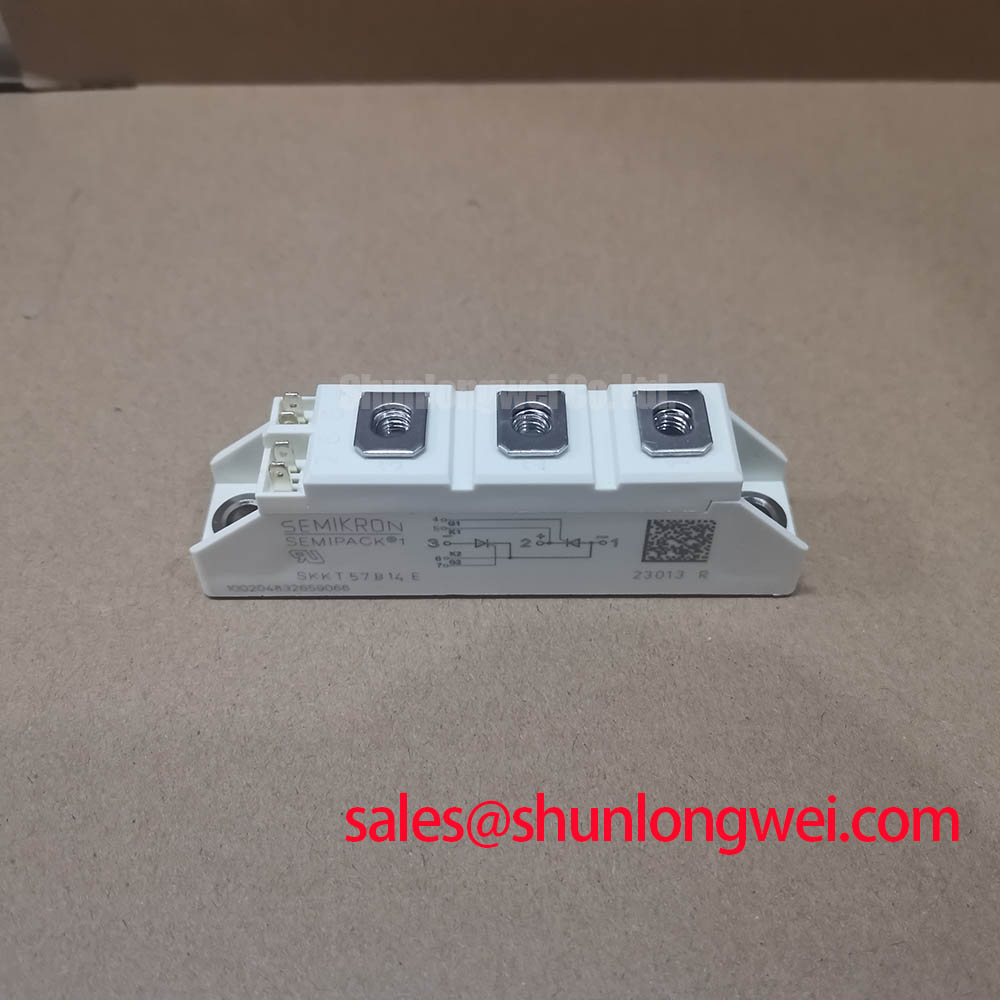
A related selection review can include VS-ST730C18L0, but electrical substitution should be based on verified voltage, current, thermal, trigger, package, and dynamic specifications rather than on physical resemblance. In a broader converter topology, an engineer may also evaluate SKKT91/08D as a separately specified rectifier or auxiliary-stage device. It should not be treated as a direct replacement without circuit-level confirmation.
VS-85HFR40 Thermal-Electrical Optimization: Junction-to-Heatsink Heat Dissipation in Practical Tuning
The operating junction temperature range specified for the VS-85HFR40 is −65 °C to +180 °C. This is an official junction-temperature boundary, not a guarantee that the installed heatsink, interface compound, enclosure, or cooling fan will maintain that condition. The stated 85 A average forward-current rating is conditioned by TC = 140 °C, so the thermal assembly must be evaluated together with the actual current waveform and duty cycle.
For a stud-mounted device, clean the mating surfaces and inspect the mounting face, nut, washer, and heatsink threads before installation. The contact area should remain flat and free from burrs, oxidation, excess compound, and trapped debris. Apply only the interface material specified by the equipment or heatsink manufacturer. Excess compound can reduce mechanical stability and contaminate adjacent insulation, while insufficient coverage can create localized thermal resistance.
Heatsink contact pressure should be uniform and applied without twisting the body or stressing the stud. Because the official information supplied for this product does not specify a mounting torque, the assembler should use the original Vishay mechanical instructions or the equipment manufacturer’s controlled work instruction. After commissioning, compare temperature rise between equivalent positions and inspect for abnormal gradients that may indicate contact or airflow problems.
Thermal assessment should include the complete path from junction to case, interface, heatsink, and ambient air. The supplied data does not state a junction-to-case thermal resistance value, so it should not be invented for calculation. Engineers should obtain the applicable thermal resistance data and then verify the result with measured case temperature, airflow condition, and load profile.
Regular cleaning is especially important in induction heating cabinets, where conductive dust, metal particles, and restricted airflow can increase thermal stress. Maintenance Note: During scheduled service, isolate the equipment, clean the heatsink and air path, inspect the interface material for drying or displacement, and compare contact temperature under a known operating load.
For assemblies using insulated substrates or more advanced cooling arrangements, the engineering background in The Advanced Thermal Management Revolution may help frame the thermal-interface review. It does not replace the device-specific Vishay thermal data or the installed equipment validation.
Field Diagnostics & Commissioning: Turn-On Current Rise Limiting in VS-85HFR40 Topologies
Turn-on stress should be investigated by observing the voltage and current at the semiconductor terminals during startup, steady operation, load changes, and fault recovery. An RC snubber can reduce unwanted voltage transitions in some topologies, while a series reactor or other current-limiting element may be appropriate in another. The values of Rs, Cs, and any reactor must be determined from measured circuit impedance, commutation behavior, pulse energy, and thermal limits.
The supplied factory specifications do not state a permitted dv/dt value, di/dt value, or surge current rating. These missing parameters are essential when evaluating unwanted current or voltage transitions, localized heating, or recovery stress. Designers should obtain them from the exact device documentation and verify the complete protection network under the intended source impedance and load.
When a control or commutation circuit is present, keep its return path separated from high-current commutation paths where the equipment layout permits. Common-mode ground movement can disturb control timing, but the corrective action must be confirmed with differential measurements at the device terminals. Shielding, filtering, pulse shaping, and control repetition should be selected by the system designer after reviewing the actual noise spectrum and control reference arrangement.
For bidirectional DC to DC battery equipment or regenerative industrial supplies, repeated thermal cycling can change terminal contact quality, interface condition, and enclosure temperature. This product page does not provide a lifetime-hour prediction or field failure rate. A maintenance program should instead trend case temperature, load current, terminal condition, cooling performance, and abnormal waveform changes over the equipment service interval.
Before returning a repaired converter to production, confirm insulation clearances, terminal polarity, fuse coordination, transient suppression, heatsink contact, and the measured operating temperature. The Vishay Industrial Power MOSFETs resource provides broader power-semiconductor context, but it does not establish the electrical limits of this diode device.