

Content last revised on September 10, 2026
Preventing Spurious Faults: Thermal Time Constants and Peak Junction Guidelines for 1MBI600U4B-120
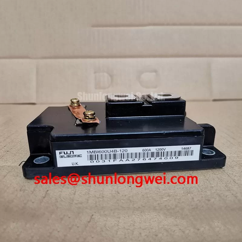
Begin incoming inspection with the power stage isolated and fully discharged: compare the module marking with the purchase record, inspect the case for cracks or deformation, and verify the stated electrical boundary of 1200 V and 600 A before connecting any test supply. The supplied product data identifies the Fuji Electric 1MBI600U4B-120 as a Module package. Terminal polarity and internal topology must be confirmed from the original Fuji documentation for the exact production variant rather than inferred from external appearance.
A cold-state bench check should use a current-limited instrument and an ESD-controlled workstation. Measure between the identified power terminals and gate terminals only after confirming the terminal map. A diode-test reading across an antiparallel path can provide a comparative screening value, but the reading is not an official acceptance limit for this module. Compare the result with a known-good unit tested under the same lead placement, polarity, meter range, and ambient conditions. An unexpectedly open or strongly asymmetric reading should lead to a second inspection for wiring, meter contact, and residual charge before any component-level conclusion is made.
💡 Bench Tip: Keep the module shorted and protected against static discharge during cold testing, and record the first reference readings before applying gate drive or power voltage.
For thermal evaluation, the important distinction is between case temperature and junction temperature. A case sensor can show a stable value while the semiconductor junction is still responding to a short overload pulse. A multi-RC thermal model is therefore a useful Engineering Calculation method: the applied loss waveform is convolved with the transient thermal impedance, then the estimated junction rise is compared with the maximum junction temperature and switching conditions specified in the applicable Fuji datasheet. The required thermal constants, steady-state thermal resistance, overload curves, and permitted pulse conditions should come from that document. They are not established by the three basic product fields supplied here.
When engineers evaluate this module in a utility-scale central photovoltaic inverter, the first compatibility question is the electrical topology. A 1200 V rated device must not be treated as a direct switching device on a 1500 V DC bus. It may only be considered where the actual isolated or clamped subsystem voltage, transient envelope, gate-drive conditions, and protection architecture remain within the verified device ratings. The system designer should measure the collector-emitter waveform at the module terminals during startup, steady switching, fault clearing, and recovery from overload.
Thermal time constants also matter during repetitive overloads. The test record should correlate collector current, switching frequency, duty cycle, case temperature, cooling interface condition, and junction-temperature estimation. ITSM or surge-current capability must not be assumed from the continuous current value of 600 A. If the original datasheet does not provide the relevant surge curve and pulse duration, the safe recovery window remains undetermined and requires manufacturer documentation or controlled qualification testing.
Mechanical installation affects the thermal result. The mounting surface should be clean, flat, and free from burrs; the thermal interface should be applied consistently; and the clamping sequence should prevent case distortion. Mounting torque is a Design Consideration governed by the module drawing, fastener type, heatsink material, and interface system. Do not substitute a generic torque value for the Fuji installation specification. After assembly, repeat the thermal test because a change in interface pressure can alter the measured case-to-heatsink temperature difference.
Transient Dynamics & Electrical Design: Cosmic Ray Robustness and Voltage Derating Considerations for 1MBI600U4B-120
Voltage-margin analysis must begin with the actual collector-emitter waveform, not with the nominal DC-link label. The supplied rating for this product is 1200 V, so a 1500 V photovoltaic inverter bus is outside the direct voltage boundary unless the module is used in a separately isolated and appropriately clamped circuit. Any proposal involving a chopper branch, clamp network, auxiliary conversion stage, or braking path requires verification of repetitive voltage, switching overshoot, fault voltage, and recovery conditions at the device terminals.
Cosmic-ray and terrestrial-neutron effects are high-risk reliability topics. A specific SEB probability, FIT rate, altitude correction, or voltage derating percentage cannot be assigned without an authoritative Fuji qualification source and a defined mission profile. Altitude, shielding, silicon technology, applied electric field, duty cycle, and system fault response all influence the assessment. The appropriate Design Consideration is to obtain the manufacturer’s qualified limits and then validate the maximum measured voltage under the intended installation conditions. The IGBT Design & Integration reference can support broader review of gate drive, thermal paths, and switching-loop behavior.
Desaturation protection should be treated as a system function rather than an assumed feature of the module. The gate driver must identify abnormal VCE behavior while accounting for blanking, sensing delay, noise immunity, propagation delay, and the actual short-circuit withstand data in the Fuji datasheet. The protection response should be validated on a controlled test bench with a current-limited DC source and a high-bandwidth differential probe. A two-stage soft turn-off strategy can reduce the rate of current interruption before the driver completes shutdown, but its timing and gate-current profile must be selected from the driver, module, and loop-inductance combination.
Long motor or inverter cables create a separate transient problem. Their distributed capacitance and inductance can produce reflected-wave behavior, causing a local peak that differs substantially from the voltage measured at the power cabinet. A filter, common-mode network, or dv/dt control stage should therefore be evaluated at the module terminals and at the remote load interface. The filter is a system-level solution, not an official parameter of the 1MBI600U4B-120. Engineers should verify insulation coordination, clamp energy, resonance, and switching loss before approving a cable configuration.
Use the Fuji Electric information on Fuji Electric Brake Chopper IGBT Modules as an external industry reference for braking-chopper application context, while confirming every voltage and current limit against the exact product datasheet. A related 2MBI150UC-120 may be reviewed as a separate reference model, but its topology and ratings do not establish interchangeability with this module.
Benchtop Waveform Tuning: Gate Loop Damping and Miller Clamp Evaluation for 1MBI600U4B-120
Gate-drive troubleshooting should start with the driver output measured directly at the module gate and emitter reference points. Measuring at the driver board alone can hide voltage differences created by common-emitter inductance, connector resistance, and gate-loop coupling. The system integrator should confirm the gate threshold, recommended drive voltage, maximum gate-emitter voltage, gate resistance range, and switching test conditions from the Fuji documentation for this exact part.
High dv/dt can transfer displacement current through the Miller capacitance and raise the opposing device gate voltage. This may contribute to cross-conduction, but the waveform must be verified rather than diagnosed from a switching fault alone. Capture both gate-emitter voltages, collector-emitter voltage, collector current, and driver supply behavior on the same time base. If the unwanted gate excursion follows the power transition, review the gate-loop return path, shared emitter impedance, probe ground arrangement, and driver source impedance before changing the gate resistor.
An active Miller clamp can provide a low-impedance discharge path when the controlled device is commanded off. Its suitability depends on the driver’s clamp threshold, sink capability, propagation behavior, isolation arrangement, and the module’s gate-charge characteristics. Negative gate bias is another possible Design Consideration, but a value such as −5 V or −15 V must not be assigned without the applicable Fuji gate-emitter limit and driver specification. The correct starting point is the manufacturer’s approved gate-drive window, followed by bench tuning under the highest measured dv/dt and worst-case temperature.
Parasitic gate inductance should be minimized to suppress ringing and false turn-on. Keep the power switching loop and gate loop physically controlled, separate high-current commutation paths from sensitive gate-return conductors, and verify the result using a short spring connection or suitable differential probe. Gate-resistor changes should be evaluated for the tradeoff between switching loss, overshoot, electromagnetic interference, and cross-conduction risk. A setting that appears stable at light load may behave differently during the current rise associated with a central inverter’s power stage.
For parallel operation, positive temperature coefficient behavior can support static current sharing in some IGBT operating regions, but it does not guarantee dynamic sharing. Each device path needs comparable busbar geometry, gate-drive propagation, thermal coupling, and emitter impedance. The engineer should measure current sharing during turn-on, conduction, turn-off, overload, and thermal steady state. No parallel count or balancing resistor value should be inferred from the nominal 600 A field alone.
Transient Dynamics & Electrical Design: SCSOA Overcurrent Protection for 1MBI600U4B-120
Short-circuit protection must be coordinated with the module’s documented SCSOA or short-circuit withstand data. The product information supplied here confirms 1200 V, 600 A, and a Module package, but it does not provide a short-circuit duration, SCSOA curve, desaturation threshold, or permitted fault repetition rate. Those limits must be taken from the exact Fuji datasheet. A protection controller should be tested against the complete response chain, including current rise, sensing blanking, driver delay, soft turn-off, fault latch, and restart inhibit.
Two-stage soft turn-off is an Engineering Recommendation that can be evaluated when a hard gate pull-down would create excessive inductive voltage. The first stage reduces gate drive or controlled gate current, allowing the commutation path to respond; the second stage completes turn-off after the driver confirms the intended fault sequence. The actual timing, gate voltage, and pull-down current are system-determined. They must be tuned with the measured stray inductance and verified against the module’s collector-emitter voltage boundary.
Fast semiconductor fuses may be coordinated with an I²t requirement, but fuse selection cannot be based on the module’s current rating alone. The engineer should compare the prospective fault current, fuse clearing characteristic, cable impedance, DC-link capacitance, and module short-circuit withstand curve. A fuse can limit energy in one fault path while leaving another path exposed through busbar coupling or a failed bypass device. Controlled fault testing should confirm that the fuse, gate driver, contactor, and clamp network operate in the intended sequence.
During field troubleshooting, inspect the gate waveform first, then the collector-emitter overshoot, current sensor output, desaturation signal, and fault-latch timing. An intermittent trip may involve noise coupling, insufficient isolation, probe error, thermal drift, or a marginal mechanical connection rather than one single failed element. Record cold and hot measurements under repeatable conditions and compare them with the known-good phase leg. Any replacement decision should also verify the original terminal arrangement, mounting interface, cooling path, gate-drive polarity, and protection interlocks before energization.