Content last revised on September 10, 2026
Mitigating Hard Switching Transients via Active Desaturation Soft Shutdown
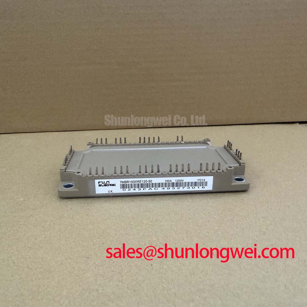
The 7MBR150VR120-50 from Fuji Electric is a 7th-generation V-Series Power Integrated Module (PIM) packaging a three-phase input rectifier, a dynamic brake chopper, and a three-phase inverter bridge into a compact footprint. Designed for demanding applications such as commercial string inverters and micro-grid battery energy storage systems (BESS), managing severe hard-switching dynamics under fault conditions represents the primary barrier to long-term power stage reliability. The module operates with an inverter rating of VCES = 1200V and continuous collector current IC = 150A (Official Datasheet Specification), alongside a maximum junction temperature rating of Tj(max) = +175°C (Official Datasheet Specification).
When operating in central or decentralized string power conversion architectures, switching events expose the silicon dies to severe short-circuit scenarios. In a Type-I short circuit, the IGBT turns on directly into an existing low-impedance line-to-line or line-to-ground fault. In a Type-II short circuit, a flashover or shoot-through event occurs while the device is already in the fully conductive on-state. Under both conditions, the collector current ramps rapidly beyond the saturation region into desaturation, causing collector-emitter voltage across the active die to rise toward the full DC-bus potential while conducting several times the rated current. According to Short Circuit Safe Operating Area (SCSOA) requirements, fault clearing must execute within a strict duration—typically under 10 microseconds (and preferably under 6 microseconds at elevated junction temperatures)—to prevent destructive thermal runaway.
| Functional Section | Key Parameter Description | Official Datasheet Specification |
|---|---|---|
| Inverter Section | Collector-Emitter Voltage (VCES) | 1200V |
| Inverter Section | Continuous Collector Current (IC) | 150A |
| Brake Section | Collector Current (IC) | 75A |
| Converter Section | Repetitive Peak Reverse Voltage (VRRM) | 1600V |
| Module Package | Maximum Junction Temperature (Tj) | +175°C |
Conventional hard turn-off during a desaturation event produces an extreme rate of current decay (di/dt). When multiplied by the parasitic loop inductance (Lσ) inherent to the DC-bus link capacitors, laminated busbars, and internal module wire bonds, this rapid di/dt generates an overvoltage spike exceeding the rated breakdown capability of the IGBT die. To suppress this fatal surge, gate drive circuitry must implement a Two-Stage Soft Turn-Off (2SSTO) mechanism. Upon desaturation detection via a high-voltage blocking diode monitoring the VCE(sat) voltage, the gate driver reduces the gate-emitter voltage (VGE) from its nominal +15V drive level to an intermediate plateau (such as +7V to +9V) for 1.5 to 3.0 microseconds. This step throttles the channel conduction and moderates the fault current slope before completing full gate discharge down to the negative cutoff rail.
The internal regenerative brake chopper section, rated at IC = 75A (Official Datasheet Specification), demands equivalent gate-drive discipline. When dynamic energy from rapid micro-grid deceleration or sudden photovoltaic array curtailment is redirected to an external braking resistor bank, fast chopper switching creates steep inductive steps. Integrating an Active Miller Clamp (AMC) on both the brake and inverter channels prevents parasitic cross-conduction. As high dv/dt appears across the opposing switch during commutation, current injects through the reverse transfer capacitance (Cres). Without a low-impedance sinking path, this displacement current charges the input gate capacitance (Cies) above the threshold voltage (VGE(th)), causing catastrophic shoot-through. Applying a robust negative bias (such as -5V to -8V) during the off-state, paired with a designated AMC transistor engaging below +2V on the gate trace, provides the required margin against common-mode ground bounce and dv/dt-induced false triggering.
Cosmic Ray Robustness: Voltage Derating Curves across 2000m-4000m Altitudes
Commercial string inverters and modular micro-grid energy storage units are increasingly installed at high-altitude mountain sites and elevated plateaus ranging from 2000 to 4000 meters above sea level. Operating power semiconductors in these environments introduces two critical engineering challenges: diminished convective air cooling due to reduced atmospheric air density, and accelerated semiconductor failure rates driven by high-energy terrestrial cosmic ray neutrons.
Atmospheric neutron flux increases exponentially with altitude. High-energy neutrons penetrating the silicon bulk collide with the lattice atoms, creating dense localized electron-hole plasma tracks. Under the influence of a high static electric field in the reverse-biased space-charge region, this plasma track can initiate an avalanche breakdown mechanism known as Single Event Burnout (SEB). SEB is an instantaneous, catastrophic failure mode that occurs without prior thermal degradation. Because cosmic ray failure in time (FIT) rates are strongly dependent on the continuous DC-bus operating voltage, systematic voltage derating is essential for high-altitude survival.
For high-voltage systems governed by standard power conversion benchmarks such as the IEC 60146 Semiconductor Converters Standard, baseline sea-level designs that operate with continuous DC-link voltages of 800V to 900V on a 1200V device must be recalculated for high-altitude installations. Field data and physical modeling demonstrate that to maintain target FIT rates (typically <100 FIT per power stage) at altitudes between 2500m and 4000m, the continuous DC-bus voltage headroom on the 7MBR150VR120-50 should be restricted to a continuous 650V–750V operational ceiling. For topologies operating on stiff 800V to 1000V DC links at high altitude, engineers often evaluate whether a modular dual-pack configuration, such as the 2MBI150-060 for segmented lower-voltage subsystems or higher-voltage discrete stages, provides better architectural partitioning.
In addition to active voltage derating, sub-cycle fault protection on the three-phase converter section—rated at VRRM = 1600V (Official Datasheet Specification)—requires strict coordination with fast-acting semiconductor fuses. The input converter diodes must endure transient line surges while matching fuse clearing ratings. The melting energy (I2t) of the AC-side fuse must remain strictly below the maximum surge current integral (I2t at 10ms half-sine) of the module's internal diode bridges. This precise coordination ensures that if an AC line surge or bridge short occurs, the semiconductor fuse isolates the sub-circuit before explosive housing rupture or case rupture occurs, protecting neighboring DC-link capacitors and control electronics.
Bi-Directional DC-DC Buck-Boost Conversion & Battery Cycling Thermal Management
In micro-grid and battery energy storage architectures, the power module frequently interfaces between a centralized high-voltage battery array and the common DC bus, executing bi-directional buck-boost power conversion. Power flows cycle between charging modes (bucking the DC bus to replenish battery energy) and peak-shaving discharge modes (boosting battery voltage into the inverter link). These operations subject the power semiconductors to dynamic power cycling at high current rates (0.5C to 2C battery charge/discharge profiles), inducing repetitive junction temperature swings (ΔTj).
The relationship between temperature cycling amplitude (ΔTj), mean operating junction temperature (Tj(mean)), and bond wire/solder fatigue is a primary factor in lifecycle reliability. Although the module is rated for Tj(max) = +175°C (Official Datasheet Specification), commercial micro-grid installations targeting a 15- to 20-year service life require the steady-state operating junction temperature to remain below +125°C, with dynamic thermal excursions (ΔTj) constrained to less than 40K per cycle. Detailed diagnostic methods and failure mode analyses for thermal-mechanical wear in power packages are comprehensively documented in the Field Engineer’s Handbook.
Achieving stable thermal impedance across the entire module baseplate requires rigorous thermal interface material (TIM) application and mechanical fastening procedures. Non-uniform TIM thickness creates localized thermal bottlenecks that accelerate center-die silicon degradation.
- Baseplate Surface Flatness: Ensure heatsink mounting surface flatness exhibits a roughness of Rz ≤ 6.3 μm and a total planarity deviation of less than 50 μm across the 100 mm mounting span.
- Thermal Compound Application: Apply a high-performance thermal grease or phase-change material using a precision screen-printing stencil to maintain a uniform wet-film thickness between 60 μm and 100 μm.
- Torque Sequence: Utilize an M5 screw fastening sequence. Initially torque all fasteners by hand or calibrated tool to a pre-tightening level of 0.5 N·m in a crisscross diagonal pattern, followed by a final uniform torque of 2.5 N·m to 3.5 N·m (General Industry Design Consideration for M5).
- Relaxation Interval: Allow a 30-minute relaxation window for phase-change or high-viscosity TIM paste to displace air pockets and achieve uniform microscopic spread before running high-current qualification sweeps.
Auxiliary Emitter Return Trace Separation for Rapid dv/dt Transients
High-speed switching in modern 1200V trench-gate IGBTs generates steep voltage and current transition rates (dv/dt exceeding 10 kV/μs and di/dt exceeding 2000 A/μs). At these speeds, even a few nanohenries of mutual parasitic inductance in the gate-emitter drive loop can distort switching behavior, generate spurious oscillations, and elevate switching losses. In large-scale power conversion frameworks, such as a Modular Multilevel Converter (MMC) in VSC-HVDC Systems, precise control of localized parasitic inductance is fundamental to avoiding unbalanced dynamic cell loading.
The 7MBR150VR120-50 provides auxiliary (Kelvin) emitter connection terminals distinct from the main high-current emitter power terminals. The physical implementation of these auxiliary connections on the gate driver printed circuit board dictates gate loop integrity.
The main emitter terminals carry the high-frequency pulsed load current. If the gate driver reference return is connected directly into the main power emitter path, the inductive voltage drop generated across the internal lead and trace inductance opposes the applied gate voltage during turn-on. This negative feedback slows the turn-on transition, dramatically increasing turn-on switching loss (Eon). During turn-off, this same inductive feedback slows collector current decay and causes uncontrolled gate oscillations that risk re-biasing the channel.
💡 Pro Tip: Always route the auxiliary Kelvin emitter terminal directly to the gate driver IC's ground pin using dedicated, closely paired differential traces parallel to the gate lead. Never tie the auxiliary emitter to the system power ground or the main DC minus copper bus on the PCB layer. The gate driver supply decoupling capacitors, gate turn-on resistor (RG(on)), gate turn-off resistor (RG(off)), and the Active Miller Clamp circuit must form a localized loop bounded exclusively by the gate pin and the auxiliary Kelvin emitter pin. Maintain a minimum creepage and clearance distance of >6.3 mm between high-voltage bus traces and low-voltage gate drive circuitry to ensure immunity against common-mode transient noise exceeding 100 kV/μs.
Implementing this layout separation guarantees that high-current load pulses flowing through the main inverter terminals exert zero inductive voltage feedback onto the sensitive gate control channel. As a result, switching transitions remain clean, symmetrical, and fully damped across the entire operating temperature and current spectrum.