


Content last revised on September 10, 2026
Assembly Integrity and Layout Architecture for 1MBI600LN-060A
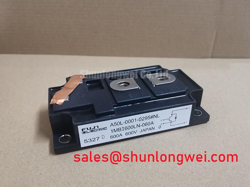
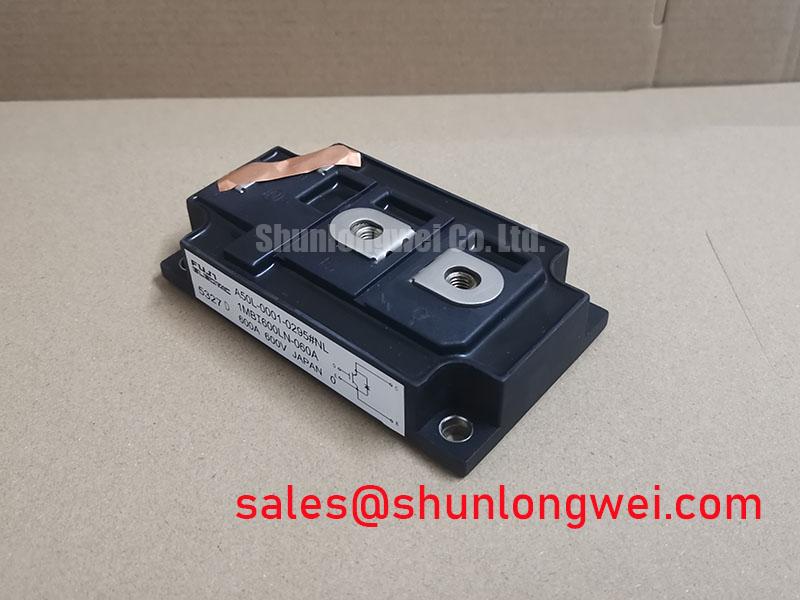
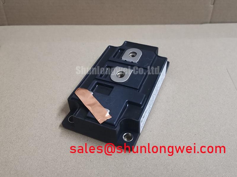
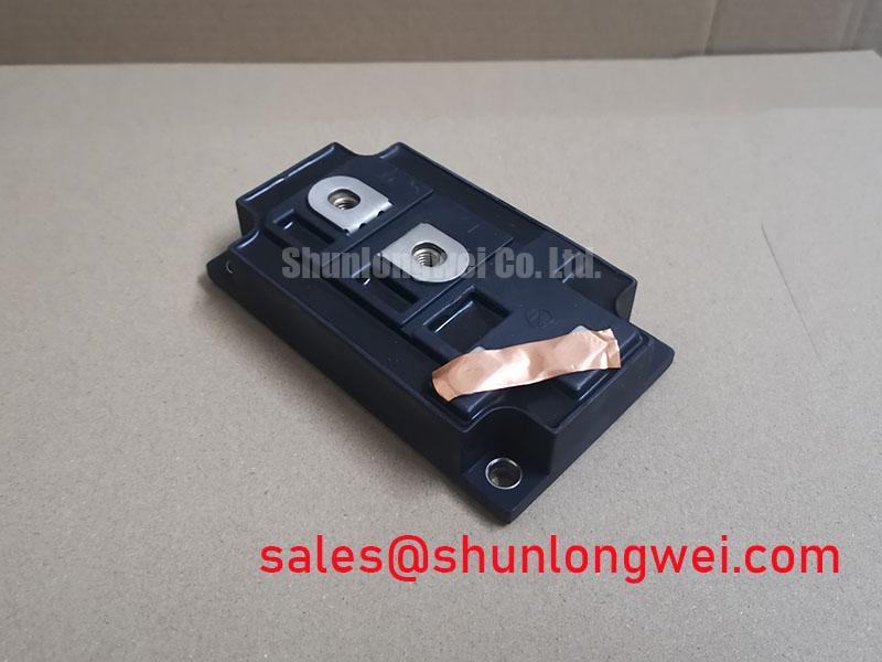
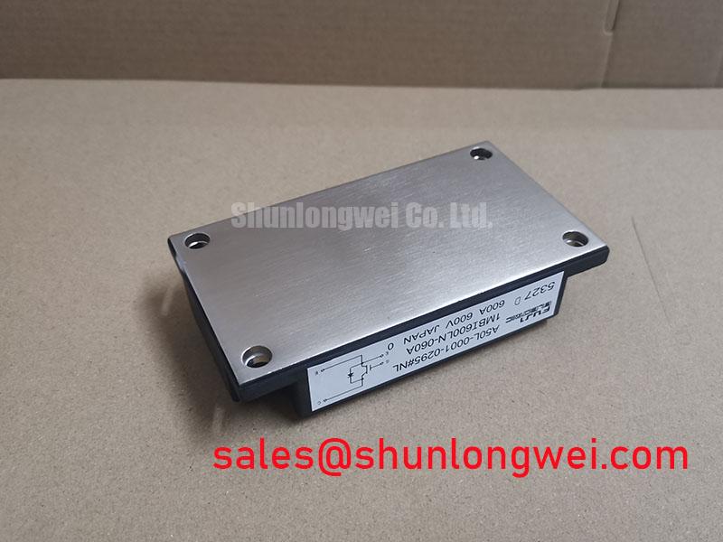
Begin incoming inspection by isolating the 1MBI600LN-060A from all energized circuits, checking the case for cracks or deformation, and confirming the nameplate against the required 600.0 V rated voltage and 600.0 A rated current. The supplied product specification identifies the package as a Module. Terminal identification should be checked against the original Fuji Electric documentation before any resistance or diode mode measurement is attempted.
For a cold static baseline, use an ESD controlled bench and a calibrated multimeter. Check the external terminals in the polarity combinations defined by the original circuit documentation, then compare the readings with a known good reference from the same equipment family. A diode mode reading can help identify an open or unexpectedly conductive path, but the result depends on the meter test current, temperature, connected circuitry, and the exact internal topology. It should not be treated as a pass or fail voltage limit unless the applicable datasheet specifies one.
In a utility scale centralized battery energy storage PCS, the module may be evaluated within a bidirectional converter power stage. System designers should verify the switching position, gate drive arrangement, current sharing method, DC bus operating range, and protection coordination from the converter schematic. The 600.0 V rating is an official specification for this product information, not a complete operating prescription for a high energy DC link. Switching overshoot, temperature, transient duty, and repetitive loading must be assessed at system level.
High altitude operation introduces additional design questions because atmospheric cooling, creepage requirements, and terrestrial neutron exposure can change with installation conditions. A specific SEB FIT rate or altitude derating value cannot be assigned here without an authoritative device reliability source and the relevant installation profile. The practical engineering method is to record site elevation, DC bus voltage, switching waveform, ambient conditions, and service history, then ask the system reliability team to evaluate the resulting margin using qualified component data.
Keep the high current commutation path compact and symmetrical where the converter topology permits. Control and power conductors should be routed to reduce unwanted coupling, while insulation spacing must be checked against the complete assembly standard rather than inferred from the module name. During troubleshooting, compare gate to emitter behavior, collector to emitter voltage, and current rise and fall on the same time base. An abnormal waveform should be investigated against the known good phase leg before replacing the device.
1MBI600LN-060A Thermal Electrical Optimization with Transient Thermal Analysis
The 600.0 A rating identifies the product category boundary supplied for this page, but actual allowable current depends on case temperature, switching frequency, conduction pattern, pulse duration, cooling hardware, and the manufacturer’s detailed electrical curves. For a battery PCS, measure the module case temperature close to the mounting surface and correlate it with phase current and switching events. A case measurement alone does not directly establish junction temperature.
Transient thermal impedance is best handled as a time dependent network rather than as a single steady state value. In engineering analysis, the selected junction to case RC network is driven by the measured or simulated loss waveform. Each pulse contributes to the thermal state left by earlier pulses, so the peak junction estimate should be checked at the most demanding operating sequence, including charge, discharge, reactive current, regeneration, and fault recovery. The RC constants and thermal impedance data must come from the applicable Fuji Electric documentation; they should not be invented from the package description.
For a practical bench correlation, calculate semiconductor losses from measured voltage and current waveforms, then compare the predicted case temperature with thermocouple or thermal imaging observations under controlled airflow. Designers should verify sensor response time and placement because a slow external measurement can miss a short overload event. If the thermal model and measurement disagree, inspect mounting flatness, interface material coverage, cooler contact, clamping uniformity, and the accuracy of the switching loss data.
Fuse coordination also requires more than matching a nominal current number. The semiconductor fuse clearing characteristic, its available fault current, and its I²t behavior should be compared with the device surge and short circuit capability specified by the manufacturer. The converter protection study should verify that the fuse, gate block, current sensor, and controller act in a coordinated sequence. A fuse that interrupts rapidly may still expose the module to a damaging first current peak if the commutation loop is inductive.
💡 Bench Tip: Discharge the DC link and wait for the equipment’s documented isolation procedure to finish before touching terminals or unplugging control wiring, then compare every cold measurement with the original phase leg reference.
1MBI600LN-060A Operational Boundaries and Short Circuit Protection
Short circuit safe operating capability is a device specific specification and should be confirmed in the Fuji Electric data for the exact revision. The available product information here confirms 600.0 V, 600.0 A, and Module packaging, but it does not provide a short circuit withstand duration, gate threshold, gate charge, or short circuit current limit. Those values must not be substituted with generic IGBT assumptions.
In a PCS, the protection chain normally combines desaturation or overcurrent sensing, gate driver response, controller fault handling, and a controlled turn off strategy. Engineers should verify the complete detection and shutdown delay under the worst current, temperature, supply tolerance, and noise conditions. A two stage soft turn off can be evaluated as a design consideration when the gate driver and module data support it, but its resistor values, timing, and gate voltage must be selected and validated by the system designer.
During a fault investigation, capture the current transformer or shunt signal, driver output, collector to emitter voltage, and DC bus waveform with suitable isolated instrumentation. Look for timing differences between healthy and affected phases, false trips during normal commutation, and voltage rise that occurs before the gate command has fully completed. These observations can indicate sensing noise, layout coupling, saturation, driver supply instability, or excessive stray inductance. They do not establish one root cause without waveform evidence.
The related 2MBI200PB-140 can be reviewed as a neutral reference for a different power semiconductor position within a broader converter or rectifier topology. It should not be treated as an automatic substitute. Voltage class, current waveform, terminal arrangement, gate drive requirements, thermal interface, and mechanical dimensions must be compared before any cross model evaluation.
Preventing Spurious Faults from Turn Off Inductive Overshoot
When current is forced to change rapidly, stray commutation inductance can add voltage to the DC bus during turn off. The engineering relationship is commonly expressed by considering the peak voltage as the DC bus contribution plus the inductive term formed by stray inductance and current slew rate. This relationship is useful for interpreting oscilloscope captures, but it does not provide a universal clamping value for this module.
Use a differential high voltage probe and a short, carefully referenced measurement loop when checking collector to emitter overshoot. Probe placement should represent the electrical terminals seen by the semiconductor rather than a remote point on the busbar. A ringing waveform should be reviewed alongside gate voltage, load current, snubber current, and the physical busbar geometry. Designers should minimize parasitic loop inductance and validate the measured peak against the module’s documented switching limits and the converter DC bus envelope.
Snubber selection is system determined. The capacitance, damping resistance, pulse energy, voltage rating, and physical location must be calculated from the measured switching waveform and validated for repetitive thermal stress. A snubber placed far from the commutation loop may have limited effect, while an oversized capacitor can increase switching current and loss. The same principle applies to laminated or symmetrical planar busbars: geometry should reduce unequal current paths, and the final result should be confirmed by measurement rather than assumed from a drawing.
For broader reliability context, engineers can consult the Power Electronics Masterclass. Fuji Electric’s resources on Brake Chopper IGBT Modules and 7th Gen X Series IGBT Modules provide useful manufacturer context, but engineers should use the exact documentation for 1MBI600LN-060A when approving voltage, thermal, switching, and protection limits.
For a neutral cross model review, the 1MBI200S-120 may be compared where the equipment documentation identifies a different electrical role. Compatibility requires confirmation of ratings, topology, gate drive behavior, protection coordination, cooling arrangement, and mechanical fit.