Content last revised on September 10, 2026
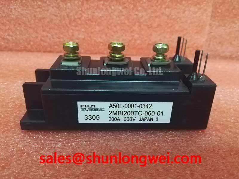
Incoming Quality Assessment and Parametric Verification for the Fuji Electric 2MBI200N-060-03 IGBT Module
Receiving inspection for power semiconductor modules demands rigorous parametric verification before installation into harsh industrial drive systems. The 2MBI200N-060-03 from Fuji Electric is a dual-pack half-bridge IGBT module designed primarily for heavy-duty variable frequency AC motor drives, uninterruptible power supplies, and regenerative braking choppers. From the perspective of incoming quality assurance (QA) and bench testing, confirming static electrical characteristics, thermal baseplate integrity, and gate isolation margins prevents catastrophic field failures downstream.
The 2MBI200N-060-03 integrates two insulated gate bipolar transistors with fast-recovery free-wheeling diodes (FWD) in a standardized half-bridge configuration. Operating on 230V to 440V AC line-rectified DC bus architectures, this device delivers high thermal and electrical stability under continuous operational stresses.
| Parameter | Datasheet Rating | Classification | Bench Measurement Conditions |
|---|---|---|---|
| Collector-Emitter Voltage (VCES) | 600 V | Official Datasheet Specification | VGE = 0 V, IC = 1.0 mA, Tj = 25°C |
| Continuous Collector Current (IC) | 200 A | Official Datasheet Specification | Continuous DC, TC = 25°C |
| Pulsed Collector Current (ICP) | 400 A | Official Datasheet Specification | 1 ms pulse width, TC = 25°C |
| Collector-Emitter Saturation Voltage (VCE(sat)) | 2.10 V (Typ.) / 2.70 V (Max.) | Official Datasheet Specification | IC = 200 A, VGE = 15 V, Tj = 25°C |
| Forward Voltage Drop (VF) | 2.30 V (Typ.) / 2.80 V (Max.) | Official Datasheet Specification | IF = 200 A, VGE = 0 V, Tj = 25°C |
| Turn-On Time (ton) | 0.60 µs (Typ.) | Official Datasheet Specification | VCC = 300 V, IC = 200 A, RG = 4.7 Ω |
| Turn-Off Time (toff) | 0.60 µs (Typ.) | Official Datasheet Specification | VCC = 300 V, IC = 200 A, RG = 4.7 Ω |
| Thermal Resistance Junction-to-Case (Rth(j-c)) | 0.155 °C/W (IGBT) / 0.350 °C/W (Diode) | Official Datasheet Specification | Per IGBT device / per FWD device |
| Isolation Voltage (Viso) | 2500 V AC (1 min) | Official Datasheet Specification | 50/60 Hz, between terminals and baseplate |
💡 Bench Tip: Before conducting curve tracer diagnostics on the 2MBI200N-060-03, always handle the module on an ESD-grounded conductive mat with a wrist strap rated at 1 MΩ resistance. Static charge accumulation on the floating gate terminals can induce microscopic oxide puncture. Use a calibrated 4-wire Kelvin digital multimeter across the main collector and emitter terminals to verify zero leakage current prior to applying gate bias.
Thermal Paste Degradation Prevention and Mechanical Clamping Torque Calibration
Heavy-duty AC motor drives expose the power stage to cyclic thermal expansions and contractions. The 2MBI200N-060-03 utilizes a nickel-plated copper baseplate engineered to transfer heat away from the silicon junctions into the external liquid or forced-air heatsink. Proper management of the thermal interface material (TIM) determines whether the rated junction-to-case thermal resistance Rth(j-c) of 0.155 °C/W (Official Datasheet Specification) is maintained over years of severe load cycling.
A frequent root cause of premature thermal breakdown in variable frequency drives is TIM degradation caused by "pump-out." Under alternating high-torque motoring and regenerative braking states, the copper baseplate flexes slightly against the rigid heatsink surface. This micro-mechanical movement displaces low-viscosity silicone grease outward, leaving micro-voids in the central area beneath the IGBT silicon dice. These microscopic air gaps elevate localized thermal impedance, accelerating thermal runaway.
To eliminate voids and control thermal impedance, apply a silicone-free, highly stable thermal grease using a screen-printing stencil or precision roller. Target a post-compression TIM wet thickness between 50 µm and 100 µm (Typical Starting Point for bench assembly). Excessively thick thermal grease increases overall case-to-heatsink thermal resistance Rth(c-s), while insufficient grease fails to fill microscopic surface roughness on the heatsink (which should maintain a surface flatness below 50 µm per 100 mm span).
⚠️ Field Alert: Fastening torque must be applied systematically. Uneven screw torque distorts the module baseplate, causing ceramic internal substrate fracture or asymmetric thermal transfer. Follow a two-stage cross-pattern fastening routine:
- Stage 1 (Pre-Torque): Hand-tighten all M5 mounting screws diagonally to approximately 0.5 to 1.0 N·m to seat the baseplate evenly.
- Stage 2 (Final Torque): Incrementally torque each M5 fastener in a cross-pattern to 2.5–3.5 N·m (General Industry Design Consideration for M5). Terminal connections on the primary bus must be tightened to 2.5–3.5 N·m using a calibrated torque wrench.
Comprehensive thermal boundaries and Safe Operating Area criteria are discussed in authoritative literature such as Electronic Design: Semiconductor Thermal Design & Safe Operating Area, which details the underlying silicon dissipation limits.
Kelvin Emitter Connection & Parasitic Inductance Minimization in High-Speed Switching
The switching performance of the 2MBI200N-060-03 features typical turn-on and turn-off intervals of ton = 0.60 µs and toff = 0.60 µs (Official Datasheet Specification). At these switching speeds, parasitic inductances inside the gate loop and the DC-link power bus create sharp transient voltage spikes and gate oscillations that can trigger unintended device turn-on.
Mutual inductance coupling between the high-current emitter path (handling up to 200 A nominal and 400 A surge) and the low-voltage gate driving loop causes severe voltage offsets during rapid current transitions. The internal Kelvin auxiliary emitter terminal of the module isolates the gate control signal return from the load current return path. Routing the gate drive return directly to this dedicated Kelvin auxiliary emitter terminal ensures that voltage drops generated by load-current rates of change (di/dt) across the power emitter connections do not subtract from or add to the applied gate-to-emitter control voltage (VGE).
For systems undergoing retrofits or legacy equipment maintenance where alternate power packaging is required, comparing pinout configurations with related parts like the 2MBI200PB-140 provides clear electrical clearance and footprint references for heavy-duty drive systems.
Layout guidelines for mitigating gate ringing and collector overvoltage spikes include:
- Laminated DC-Link Busbars: Utilize wide, closely spaced copper plates separated by thin insulation to minimize DC bus parasitic inductance below 30 nH.
- Gate-Emitter Twisted Pair Routing: Twist gate and auxiliary emitter lead lines tightly, keeping track lengths below 10 cm to limit radiated noise pickup from adjacent phase conductors.
- Direct High-Frequency Snubbers: Mount polypropylene film snubber capacitors directly across the primary positive and negative DC terminals of the module to absorb turn-off inductive kicks.
- Dead-Time Margin Settings: Set inverter dead-time to a minimum of 1.5 µs to 2.0 µs (Design Consideration for 600V modules) to prevent bridge shoot-through conditions caused by carrier storage delays.
Evaluating Thermal Capacitance vs Heat Sink Time Constant under Surge Bursts
In variable frequency motor control, industrial machinery often demands brief, intense overload currents during motor startup, rapid deceleration, or mechanical jamming. Under high transient loads, the silicon junction temperature Tj rises far more rapidly than the heatsink temperature because the thermal capacitance of the silicon die and copper baseplate is orders of magnitude smaller than the massive thermal inertia of an external extruded heatsink.
Evaluating this dynamic thermal stress requires analyzing transient thermal impedance Zth(j-c) rather than relying solely on steady-state thermal resistance. The thermal response of the 2MBI200N-060-03 can be evaluated using multi-stage RC network representations (Foster or Cauer thermal models) where each internal layer—silicon die, solder layer, ceramic DCB (Direct Copper Bonded) substrate, baseplate, and TIM—presents distinct thermal resistance and thermal capacitance constants.
During a 100 ms motor acceleration surge at double the nominal current (400 A), thermal energy concentrates primarily within the silicon and ceramic substrate layers. The heatsink remains relatively cool during this millisecond window. If repetitive surge bursts occur without adequate recovery time, junction temperatures can exceed the maximum operating junction temperature limit (typically 150°C), triggering bonding wire fatigue and solder delamination.
Technicians and field service personnel looking to benchmark degradation signatures, thermal fatigue cycles, and parametric screening standards can refer to practical inspection guides in the Field Engineer’s Handbook.
When bench testing incoming units for static conduction health, measure the collector-emitter saturation voltage VCE(sat) with a short, low-duty pulsed current source (e.g., 200 A at 300 µs pulse width). A fresh, undamaged 2MBI200N-060-03 must exhibit a forward saturation voltage around 2.10 V typical (Official Datasheet Specification) at Tj = 25°C. Deviations exceeding 15% from factory typical values generally indicate internal die mismatch or bonding degradation.
Common-Mode Transient Immunity (CMTI > 100kV/µs) in Harsh Industrial Environments
Variable frequency drives switching continuous phase currents of 200 A at high DC bus voltages generate steep voltage gradients (dv/dt) across the half-bridge output node. These fast transitions introduce high-frequency displacement currents through stray parasitic capacitances across the gate driver galvanic isolation barrier.
Common-Mode Transient Immunity (CMTI) defines the capability of the gate driver isolation barrier to withstand rapid ground-potential shifts without corrupting the logic control states. In modern industrial motor drives, high CMTI ratings (exceeding 100 kV/µs) are essential to prevent false gate triggering. When the low-side IGBT turns on rapidly, the high-side floating reference potential drops abruptly at rates that can exceed 10 kV/µs. If displacement currents pass through the isolation barrier capacitance (Cio), they can induce transient spikes on the driver output, turning on the high-side IGBT while the low-side device is active, causing a direct DC bus short-circuit.
Protective circuit implementations to counter common-mode noise and gate disturbances include:
- Active Miller Clamping: Connect an active Miller clamp circuit directly to the gate pin. When the gate voltage drops below approximately 2.0 V during turn-off, the clamp provides a low-impedance path to ground, bypassing the gate resistor and sinking Miller-effect displacement currents.
- Negative Gate Turn-Off Bias: Apply a negative gate drive bias (e.g., -5 V to -10 V) during the OFF state rather than a simple 0 V bias. This provides a robust safety margin against positive-going common-mode noise spikes exceeding the gate threshold voltage VGE(th).
- Galvanic Isolation Integrity: Implement gate drive optocouplers or digital magnetic/capacitive isolators that feature guaranteed isolation ratings exceeding 2500 V AC, ensuring complete galvanic separation between the industrial MCU and high-voltage power switching nodes.
In high-power architectures requiring alternative topologies or higher bus voltage ratings, engineers often evaluate matching or complementary components such as the 2MBI200UD-120-51 to satisfy system voltage headroom and isolation requirements.
Benchtop Diagnostic and Incoming QA Inspection Procedure
To ensure total reliability before mechanical assembly, execute the following three-step static parameter check on the 2MBI200N-060-03 using standard lab equipment: