Content last revised on October 24, 2026
6MBP150RA120 Operational Boundaries: Evaluating Regenerative DC-Bus Voltage Limits
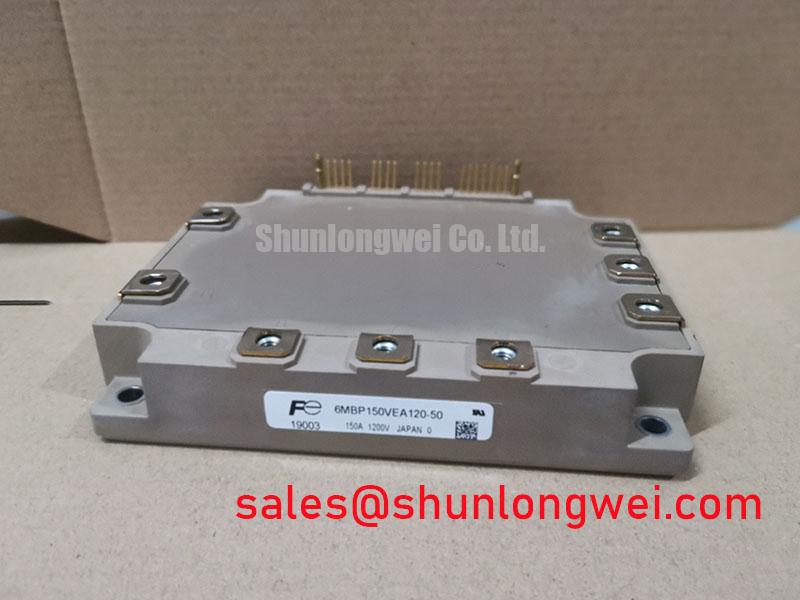
When a heavy-duty variable-frequency AC motor drive reports a DC-bus overvoltage or regenerative braking fault, isolate the power stage, verify the DC-link discharge state, and inspect the module connections before applying any control signal. The 6MBP150RA120 from Fuji Electric is an intelligent power module (IPM) with integrated drive and protection circuitry. It is specified with a 1200 V collector-emitter voltage and a 150 A continuous collector current at TC = 25°C, making its electrical limits directly relevant to mid-power industrial inverter service.
The listed VCE(sat) is 3.0 V maximum under the specified test conditions, while the over-heating protection temperature is approximately 150°C typical. The module also carries an isolation voltage of 2500 V AC for one minute. These specifications should be separated from system-level design targets, which depend on switching frequency, motor load profile, cooling arrangement, DC-link control, and control-interface implementation.
| Specification | Value | Engineering Significance |
|---|---|---|
| Collector-emitter voltage, VCES | 1200 V | Establishes the rated blocking-voltage boundary for the IGBT switching stage. |
| Continuous collector current, IC | 150 A at TC = 25°C | Supports evaluation in industrial motor-drive power stages subject to thermal and switching conditions. |
| Collector-emitter saturation voltage, VCE(sat) | 3.0 V maximum under the specified test conditions | This value is used when estimating conduction loss at the specified test conditions. |
| Over-heating protection temperature, TjOH | Approximately 150°C typical | Provides a thermal protection reference for the module’s protection behavior; it does not establish the temperature of every IGBT junction. |
| Isolation voltage, Viso | 2500 V AC for 1 minute | Defines the stated dielectric withstand capability under the manufacturer's specified isolation test conditions. |
Regenerative braking must be assessed by observing how the motor’s returned kinetic energy raises the DC-link voltage, rather than by sizing a braking path from motor power alone. During deceleration, the inverter may transfer energy back into the DC bus faster than the line-side converter or load can absorb it. Where fitted, a separate braking switch and ballast resistor provide a controlled dissipation path. The 1200 V VCES rating of the 6MBP150RA120 remains one boundary for the inverter stage; it does not specify the ratings of the separate braking circuit.
For a repair assessment, capture the DC-link voltage during the exact deceleration event that produces the fault. The measurement should include the highest transient peak, the duration of the rise, the braking command state, and the thermal condition immediately before the event. A meter reading taken after the fault may show an acceptable average voltage while missing the short overshoot that stresses the IGBT. Use an appropriately rated differential probe and confirm the probe connection, bandwidth, and grounding method before energizing the drive.
The ballast resistor must be evaluated for pulse energy, repetition rate, cooling, and connection inductance. A resistor that survives one emergency stop may still accumulate excessive temperature during repeated braking cycles. The braking transistor also experiences a relationship between conduction duration and junction temperature. The module’s typical TjOH of approximately 150°C should be treated as a protection reference, not as a preferred continuous operating target or as protection for a separate braking transistor. Designers should establish the thermal response of the complete module, heatsink, interface material, airflow path, and enclosure.
Layout has a direct effect on the voltage seen by the braking switch. Keep the high-current path between the DC bus, braking device, and resistor compact and arranged to reduce loop area. Avoid routing the braking conductor beside sensitive control wiring for long parallel distances. The physical clearance around the high-voltage bus, resistor terminals, and module power terminals must be determined from the working voltage, pollution environment, enclosure construction, and applicable safety rules. These are Design Considerations rather than Fuji Electric output specifications for this particular part.
If the braking command appears late, check the DC-link sensing path, comparator or controller timing, gate-driver supply behavior, and the resistor contactor or switching interface where fitted. If the fault occurs only after repeated deceleration, compare the heatsink temperature and braking-resistor temperature across the duty cycle. A replacement evaluation should also compare terminal geometry, isolation arrangement, protection interface, and drive requirements rather than relying on voltage and current ratings alone. The 2MBI300VW-120D-51 may be reviewed as a related power-module reference, but its dual-IGBT configuration differs from this six-switch IPM. Electrical, mechanical, and control compatibility must be established by the system engineer.
6MBP150RA120 Circuit Protection & Reliability: Mitigating Commutation Voltage Spikes
Switching voltage stress is shaped by commutation current, stray inductance, diode reverse recovery, gate timing, and the impedance of the DC-link connection. In a three-phase motor inverter, the freewheeling path can produce a reverse-recovery current peak when the complementary IGBT turns on. A sharp recovery event increases di/dt and can produce voltage overshoot and ringing through parasitic inductance.
Use a high-bandwidth voltage probe with suitable differential and common-mode ratings at the module terminals when evaluating this behavior. Probe placement should represent the actual electrical loop, because a long measurement lead can add ringing that does not exist at the semiconductor terminals, while an unsuitable ground connection can conceal or exaggerate the event. Compare turn-on and turn-off waveforms at several load currents and operating temperatures. The purpose is to identify whether the voltage peak follows the commutation event, the switching transition, or a control-side disturbance.
An RC snubber can reduce high-frequency ringing by providing a local transient current path, but its values are system-dependent. The snubber must be selected from measured ringing frequency, damping behavior, power dissipation, capacitor pulse capability, and physical placement. It should not be treated as a universal accessory value for the 6MBP150RA120. Place the snubber loop close to the switching terminals when the mechanical construction permits, and verify that its connection does not add a larger current loop or compromise creepage and clearance.
Gate resistance is an adjustment point in power stages with externally accessible gates. Increasing turn-on resistance can reduce switching speed and peak recovery current, but it also changes switching loss and may affect the thermal balance of the inverter. The 6MBP150RA120 incorporates its gate-drive circuitry, so this should not be treated as an available external adjustment. Evaluate its switching behavior using the manufacturer's specified control interface, supply conditions, and application guidance.
The module’s 3.0 V maximum VCE(sat) is useful for conduction-loss assessment at the specified test conditions, but it does not describe turn-off overshoot or reverse-recovery behavior. Those transient conditions require waveform measurement under the intended supply and load arrangement. The same principle applies to electromagnetic compatibility: a lower ringing amplitude at the module terminals can reduce one noise source, but the complete drive still requires enclosure, cable, grounding, and filter evaluation. A power module should not be described as independently certified to a complete equipment EMC standard.
Verify the module’s control-supply arrangement throughout the full switching sequence. Where the system uses a bootstrap supply, its capacitor, charging diode, supply-current demand, and high-side duty cycle must retain adequate voltage under the actual operating pattern, and the arrangement must be supported by the module’s application requirements. The required supply voltage and undervoltage-protection behavior should be taken from the module documentation, not inferred from its collector rating. The related 7MBR100VN120-50 can be examined as a different power-module configuration when mapping the complete converter topology; its circuit configuration and drive requirements must be checked separately.
For reliability screening, inspect the turn-off waveform for repeated overshoot or oscillation that changes with temperature. Correlate these observations with bus voltage, motor current, and switching frequency. If a protection trip appears intermittent, check connector contact integrity, auxiliary supply stability, and probe reference integrity before replacing the power module. These checks help distinguish a commutation problem from a control or measurement fault without assigning a single cause to one symptom.
6MBP150RA120 Operational Boundaries: Managing Control Wiring and Switching Interference
The control wiring should be routed so that its return does not share the high-current power path. Reference each control input to the corresponding control-supply return specified by the module documentation. This arrangement reduces coupling between switching current and the control signal, helping the integrated driver receive a cleaner command during rapid collector-current change.
At the machine, trace the control conductors to the module terminals and identify where the signal path runs beside the collector bus, power emitter, or another phase leg. Keep the signal and corresponding return conductors close together, minimize loop area, and avoid routing them through a region carrying pulsed braking or commutation current. The physical implementation must also respect the module’s terminal arrangement and insulation requirements. A compact loop alone is not sufficient if it creates inadequate clearance from the DC bus.
Control interference can be investigated by observing the input waveform directly at the module, not only at the controller board. Look for ringing, false input transitions during the opposite switch transition, or an input voltage that differs substantially between low-current and high-current operation. The control supply should be observed at the same time because supply impedance and local decoupling can influence the apparent input waveform. Internal gate-emitter waveforms should not be assumed accessible through the module’s control terminals.
The Miller effect couples collector-voltage movement into the gate circuit through the device’s transfer capacitance. In a power stage with a separate gate driver, designers may evaluate source and sink capability, gate-clamp behavior, and turn-off impedance. For the 6MBP150RA120, follow the integrated driver’s documented operating requirements and the system’s dead-time requirements. External Miller clamps or negative gate bias should not be applied to the module’s control inputs.
💡 Pro Tip: Keep the control-signal return separate from the main high-current routing, then verify the input waveform and collector-emitter peak during a controlled switching test before releasing the layout.
Thermal and electrical checks should be performed together because switching conditions affect both loss and voltage stress. Compare phase-leg behavior under matched operating conditions, paying attention to asymmetry between channels. If one channel shows a different switching transition, inspect its control input, connector interface, control-return routing, and local supply decoupling before concluding that the IGBT itself is the source.
For engineers developing a broader verification plan, the IGBT Design & Integration reference provides related guidance on gate drive, thermal management, and converter topology. Test planning can also be aligned with relevant semiconductor qualification and testing principles published by JEDEC Global Standards for the Microelectronics Industry. The final acceptance limits remain system-defined and should be checked against the module’s documented limits and the drive’s DC-link voltage, switching waveform, thermal profile, insulation arrangement, and operating duty.