Content last revised on September 16, 2026
Benchtop Waveform Tuning: Mitigating Stress via AC Input Transient Overvoltage Clamping in 2DI100D-100
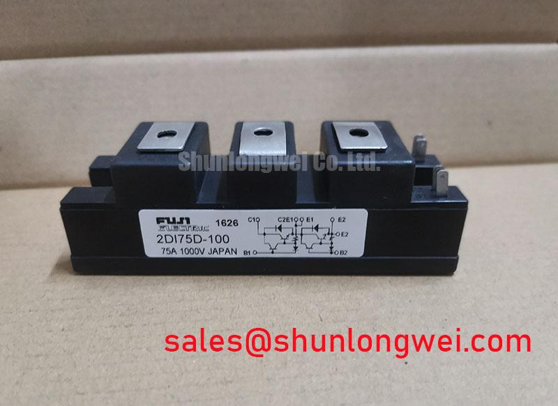
With the circuit isolated and discharged, verify the nameplate against the original equipment documentation before connecting a meter across the diode paths or reconnecting power terminals. The Fuji Electric 2DI100D-100 is specified as a diode module with a 1000 V voltage rating and 100 A current rating. Its published values should be treated as device limits, not as confirmation that the surrounding protection network, heatsink, fuse, or control cabinet remains serviceable.
| Official Datasheet Parameter | Rated Value |
|---|---|
| Specified Voltage Rating | 1000 V |
| Specified Current Rating | 100 A |
| Maximum Power Dissipation, PC | 800 W |
| Isolation Voltage, Viso | 2500 V AC for 1 minute |
Before investigating a suspected diode module fault, inspect the AC input protection chain as a complete path: incoming fuse, surge suppression element, snubber network, busbar joints, and the terminals associated with the module. A clamp that has changed condition, a loose power connection, or a degraded RC network can alter the waveform applied to a rectifier assembly even when static diode checks appear acceptable.
The 1000 V voltage rating is an official specification and is a key limit to compare against measured operating and relevant repetitive reverse-voltage conditions. MOV and RC snubber selection is a Design Consideration determined by the AC source, surge environment, upstream thyristor arrangement, wiring inductance, and measured clamp response. The published values supplied for this module do not state an MOV rating, fuse I²t coordination value, or transient surge-current rating. Those characteristics must therefore be verified from the original system documentation and by waveform testing, rather than inferred from the 100 A current rating.
For equipment assessed against surge conditions associated with IEC 61000-4-5 practices, confirm the protection architecture at the equipment level. A diode module alone is not evidence of surge or EMC compliance. Fuji Electric’s power semiconductor product information provides useful family context, while the installed assembly documentation remains the reference for this part’s terminal arrangement and protection design.
Benchtop Waveform Tuning: Mitigating Stress via Thermal Avalanche Margins during High-Peak Events on 2DI100D-100
Do not treat the continuous current figure as a substitute for an unlisted half-cycle surge capability. The official data provided for the 2DI100D-100 identifies a 100 A current rating and 800 W maximum power dissipation, but it does not provide an ITSM rating, a 10 ms surge-current curve, or an avalanche-energy rating. Any claim of permissible high-peak or thermal-avalanche operation would exceed the published information.
When an AC fault or capacitor switching event is suspected, capture current and voltage at the module connection points, then compare the evidence with the known system topology. Check whether the event coincides with fuse operation, contactor sequencing, capacitor-bank switching, or an upstream thyristor control issue. A reverse-voltage reapplication concern should be assessed through measured waveform recovery and the thermal condition of the complete power stack.
Regenerative braking choppers and bidirectional DC-DC battery systems often require careful thermal-cycle assessment, but this diode module should not be represented as the active switching device in those circuits without a verified schematic. Where it is used as part of a rectification or freewheel path, engineers should assess repetitive current loading, cooling contact, and commutation conditions using the original converter design.
2DI100D-100 Thermal-Electrical Optimization: Phase-Controlled Rectification and Firing-Angle Practical Tuning
A diode module has no firing-angle control function. In a phase-controlled rectifier, the firing angle belongs to the upstream thyristor gate-control system, while the diode path conducts according to circuit polarity and commutation conditions. For this reason, changes across a firing-angle range cannot be assigned to the 2DI100D-100 itself. DC output, displacement power factor, reactive-power demand, and capacitor-bank response remain system-determined outcomes.
For grid-tied static var compensator or thyristor-switched capacitor maintenance, verify the module’s voltage class, current rating, terminal layout, isolation requirement, and heatsink interface against the removed unit and circuit documentation. The 2500 V AC for 1 minute isolation voltage is an official specification, but it does not define the insulation coordination of the complete cabinet.
If the repair record identifies 2DI100D-050C as a related device, it should be evaluated only after confirming its own official ratings and physical interface against the original assembly. A part-number similarity alone does not establish interchangeability in a high-voltage reactive-power system.
Preventing Spurious Faults: Junction-to-Heatsink Heat Dissipation Guidelines for 2DI100D-100
Inspect the heatsink contact face for trapped debris, uneven thermal compound transfer, corrosion, and signs that mounting pressure was not distributed evenly. The supplied official information gives a maximum power dissipation of 800 W, but it does not state junction-to-case thermal resistance, mounting torque, screw size, or thermal-compound thickness. These mechanical details must be taken from the module drawing and the host equipment service procedure.
💡 Pro Tip: Tighten power-module mounting hardware in the documented cross-pattern sequence and verify that the heatsink surface is clean before applying power.
Uneven contact can raise thermal stress locally and may contribute to intermittent thermal protection trips or changing conduction behavior under load. This possibility should be checked through temperature observation, terminal inspection, and controlled load testing rather than assumed from one electrical symptom. Minimize parasitic loop inductance around power connections to suppress switching-related overshoot where the surrounding converter contains active switches, then verify peak voltage margins against the DC-link voltage during switching tests.
For broader context on loss mechanisms and switching behavior in industrial drive assemblies, see Unlocking Efficiency in Industrial Drives. That discussion supports system-level investigation, while the final thermal and electrical acceptance of this diode module must remain tied to the verified equipment schematic and measured operating conditions.