


Content last revised on September 18, 2026
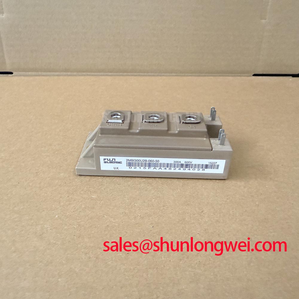
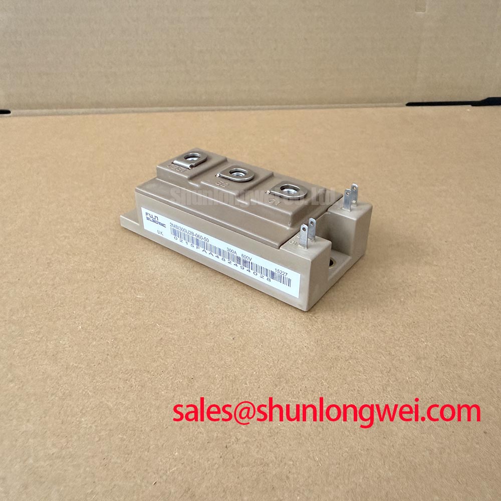
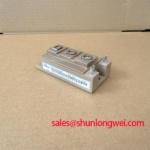
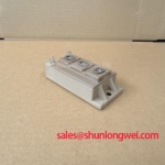
| Manufacturer | Fuji Electric |
|---|---|
| Product Type | IGBT Power Module |
| Model | 2MBI300U2B-060-50 |
| Collector Emitter Voltage | 600 V Official Specification |
| Rated Current | 300 A Official Specification |
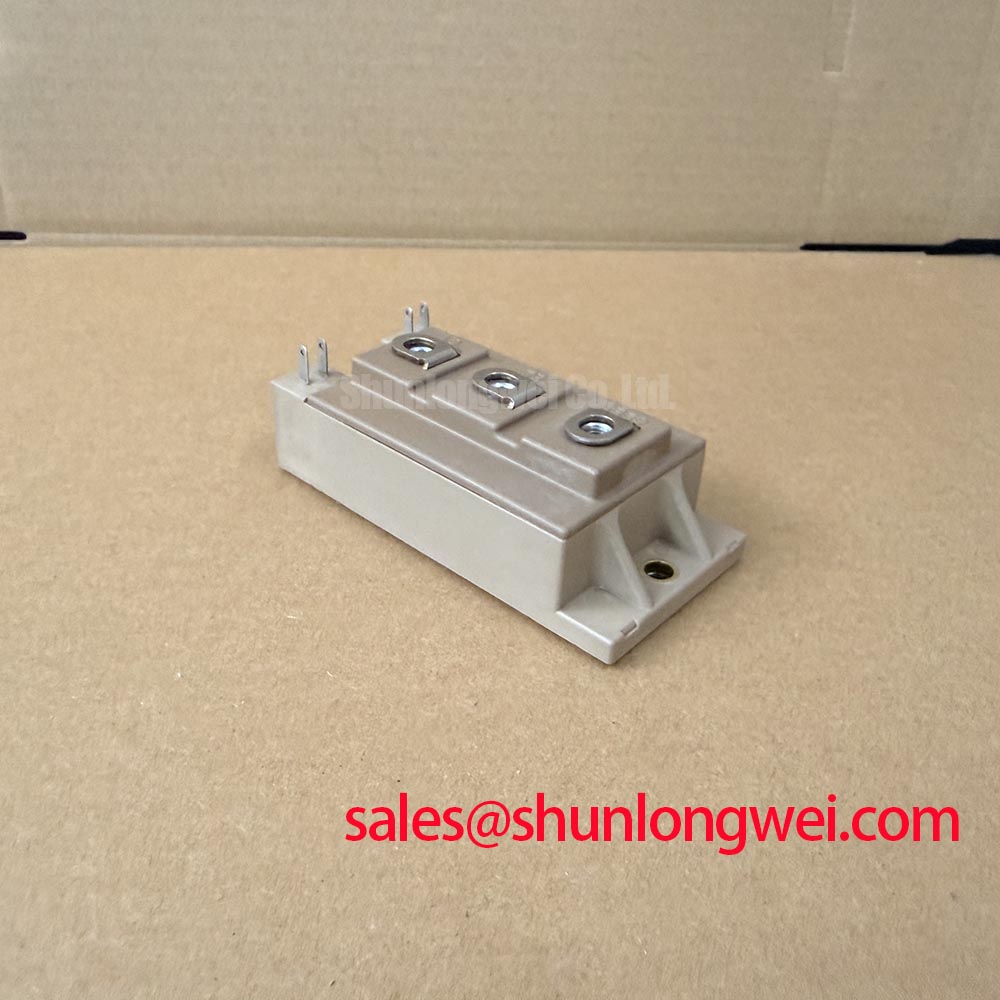
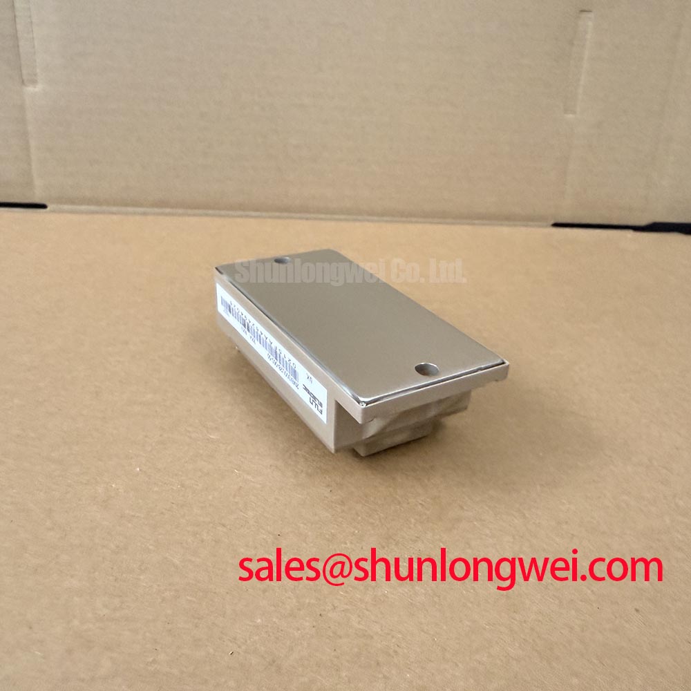
| Package | Fuji Power Module |
2MBI300U2B-060-50 Operational Boundaries: Evaluating Static and Dynamic Current Distribution AC Limits
Measure the cold resistance path between the main power terminals with the drive wiring disconnected, then compare the reading and diode response against the corresponding healthy phase or known working power section. A hard short, an unexpectedly open path, or a large mismatch between comparable inverter legs can indicate that the power stage requires deeper isolation before a replacement module is fitted.
The 2MBI300U2B-060-50 is rated at 600 V collector emitter voltage and 300 A current under its official factory specification. Those ratings define the module identity and provide the first electrical boundary for equipment repair assessment. They do not, by themselves, establish the safe DC bus level, overload duration, switching frequency, cooling capacity, or gate drive conditions of a particular inverter welder or medium frequency induction heating power supply.
For parallel current paths, static sharing and dynamic sharing must be treated as separate checks. Static sharing is influenced by the positive temperature coefficient behavior associated with IGBT saturation voltage at suitable current levels. As one conduction path becomes warmer, its conduction characteristic can tend to redistribute current toward a cooler parallel path. This is a Design Consideration, not a guarantee that separate modules will share current correctly under all operating conditions.
Dynamic current sharing depends much more heavily on gate loop symmetry, busbar geometry, driver propagation delay, and individual switching conditions. During a field repair, inspect whether the gate and emitter control wiring follows equivalent physical routing for paired power positions. A longer return path, a loose auxiliary connection, or a changed gate resistor can alter switching behavior even when the main terminals appear correctly mounted.
Oscilloscope verification should compare gate emitter voltage, collector emitter voltage, and phase current under controlled operating conditions. A current imbalance that appears only during transitions may indicate unequal loop inductance, different gate damping, or inconsistent driver behavior rather than a static module defect. Keep the power loop compact to reduce inductive overshoot during turn off, and validate peak voltage margin against the actual DC link during switching tests.
Mechanical alignment matters as much as electrical symmetry. Main terminals should sit flat against clean conductive interfaces without strain from rigid busbars or cable lugs. A terminal that is pulled sideways during tightening can create an unreliable contact surface and uneven current distribution. ⚠️ Field Alert: Isolate stored DC link energy before removing control or power connections, and tighten hardware according to the equipment manufacturer’s fastener specification with thermal compound spread uniformly across the mounting interface.
Where an equipment design is being reviewed against another Fuji Electric power module family, the 2MBI300U4E-120 can serve as a neutral reference point for comparing voltage class, current class, package arrangement, terminal layout, and drive requirements. Such comparison is an engineering evaluation exercise, not an automatic substitute decision. The system engineer should verify electrical ratings, mechanical fit, gate drive behavior, thermal path, and circuit topology before any interchange is attempted.
Transient Dynamics & Electrical Design: Output Sinusoidal Filter vs dv/dt Reactor on 2MBI300U2B-060-50
Probe the inverter output terminal and the motor end of a long cable with properly rated differential measurement equipment to identify ringing, reflected waveforms, and abnormal collector emitter voltage excursions. A waveform that is acceptable at the module terminals can look very different at a remote motor or induction heating load because cable impedance and load impedance may not match.
Long motor leads can create transmission line reflections that raise terminal voltage toward approximately twice the DC link voltage in unfavorable conditions. This is a system level Design Consideration, not an official overvoltage rating of the 2MBI300U2B-060-50. The module’s official voltage rating remains 600 V; the actual operating peak must be measured and assessed against the complete switching environment.
A dv/dt reactor and a sinusoidal output filter solve different problems. A reactor is commonly evaluated when the goal is to moderate current rise and reduce the sharpness of voltage transitions. A sinusoidal filter is usually considered where the load needs a more sinusoidal waveform or where cable length and motor insulation stress require more extensive waveform conditioning. Selection depends on output frequency, cable properties, motor characteristics, load current, and the inverter’s switching pattern.
In inverter welder repair, rapid current changes can expose weak DC bus snubbers, aged MOV protection parts, loose laminated busbar connections, or incorrect gate drive timing. In medium frequency induction heating equipment, resonant tank conditions and cable layout can introduce another source of circulating energy. Inspect MOVs for heat marks, cracking, or changes in physical condition, but do not assume that a visually normal MOV has retained its original clamping behavior. Verify the surrounding suppression network with suitable test methods and compare captured switching waveforms with known stable operation where available.
Desaturation protection belongs to the gate driver and system control architecture, not to the published core rating of this module. A protection path designed to recognize an abnormal rise in collector emitter voltage within a short, validated response time can reduce exposure during a short circuit event, provided that sensing blanking, noise immunity, fault logic, and driver response are validated in the actual equipment. Two stage soft turn off can also limit the severity of an abrupt interruption by controlling the turn off transition rather than forcing an uncontrolled current collapse.
Gate drive behavior should be checked for Miller induced turn on when the opposite switch changes state. Gate collector capacitance and the driver’s return impedance can couple a transient into a device that is intended to remain off. An active clamp arrangement may be evaluated where the system architecture supports it, but clamp threshold, gate voltage range, driver isolation, and transient response must be established through equipment level testing. Fuji Electric’s discussion of Evolution of Negative Off-Bias Gate Drive Circuits provides useful context for reviewing unwanted turn on control in high energy switching circuits.
For broader semiconductor switching background, consult Fuji Electric’s high speed IGBT technical information. The device level principles discussed there should be applied only after the complete module, driver, busbar, load, and protection arrangement have been evaluated together.
2MBI300U2B-060-50 Circuit Protection & Reliability: Calibrating Thermal Cycling Margins of Internal Braking
Measure the DC link voltage during commanded deceleration or power reduction and observe whether it rises beyond the normal operating region before assigning the failure to the IGBT module. A rising bus can result from regenerative load energy, an inactive braking path, an incorrectly controlled braking transistor, a degraded resistor connection, or a control sequence issue.
The supplied official specifications identify the 2MBI300U2B-060-50 as a 600 V, 300 A Fuji Power Module. They do not establish that this module contains an internal braking IGBT or braking resistor. Equipment designers and service teams should identify the actual braking circuit from the inverter schematic, power board layout, and connected DC link hardware before diagnosing a deceleration fault.
In a typical regenerative inverter arrangement, motor deceleration energy raises the DC link voltage. A braking IGBT, whether placed internally within a larger assembly or implemented as an external circuit, can route that energy into a high power resistor when commanded by the control system. The resistor, switching device, thermal mounting, wiring clearance, and control threshold must be evaluated as one energy handling path. Replacing only the main power module without examining this path can leave the original failure condition active.
Look for loosened resistor terminals, darkened insulation, heat affected solder joints, damaged gate driver connectors, and unequal mounting pressure on power devices. These findings may indicate repeated thermal stress, but they do not prove a single root cause. Measure the control signal at the braking device, monitor the bus response, and verify that the resistor remains electrically continuous under safe isolated test conditions.
Thermal cycling is influenced by the amplitude and repetition of temperature change across the module mounting stack and associated conductors. A clean, flat heatsink interface supports consistent heat transfer. Excess thermal compound, hardened compound, trapped debris, and uneven fastener loading can increase thermal resistance and create local mechanical stress. This is a Design Consideration based on general power module assembly practice rather than an official mounting specification for this model.
When reviewing a braking network, avoid selecting a resistor or switching device solely from nominal current. The relevant operating conditions include stored mechanical energy, deceleration sequence, repetition rate, DC link capacitance, ambient temperature, cooling path, and fault response. The system engineer should determine the required energy capability through measured operating cycles and controlled validation, rather than applying a generic resistor value or assumed overload margin.
For field replacement work, inspect the isolation spacing around the braking circuit and DC link conductors after mechanical reassembly. Conductive debris, displaced cable shields, or compressed insulation can create an unintended fault path that only appears when the bus is energized. Confirm that all gate drive connectors are fully seated and that the signal reference path has not been altered during service.
2MBI300U2B-060-50 Operational Boundaries: Evaluating Transient Thermal Impedance Limits
Capture the load current, case temperature trend, and switching waveform during the pulse sequence that produces the thermal alarm or repeated shutdown. A stable cold resistance test does not reveal whether the module is being pushed by short, repetitive energy pulses that exceed the available thermal path during real operation.
The 2MBI300U2B-060-50 carries official ratings of 600 V and 300 A, while the usable thermal margin in equipment depends on losses generated during conduction and switching, the pulse profile, heatsink condition, airflow or liquid cooling performance, and mounting quality. Current rating alone cannot predict junction temperature during a pulsed welder output or an induction heating cycle.
Transient thermal impedance is commonly represented with a multi resistance capacitance model because heat does not move through the module and heatsink instantaneously. During a short high current pulse, the junction temperature can rise faster than the case temperature sensor responds. During a longer pulse train, heat progressively reaches the case, interface material, heatsink, and surrounding cooling system. Engineers can use the applicable manufacturer thermal data to estimate the temperature rise from power loss and transient impedance, then compare the estimated junction condition with the permissible device boundary.
This is an Engineering Calculation only when it uses verified module loss data, switching conditions, thermal impedance curves, measured case temperature, and the actual cooling arrangement. It should not be replaced by a generic temperature estimate. The switching losses of a repaired inverter can change materially if gate timing, snubber condition, bus inductance, or load resonance differs from the original equipment state.
Check the heatsink surface for flatness, oxidation, embedded particles, and evidence that the module base did not make uniform contact. Inspect fastener engagement and the surrounding support structure for distortion. In assemblies using disc springs or pressure controlled mounting hardware, the spring orientation and compression condition should be restored exactly as intended by the equipment design so that pressure is distributed consistently across the mounting surface.
For double sided cooled assemblies or tightly packed power stacks, confirm that both cooling interfaces are seated before energization. Uneven clamping can create a temperature imbalance that is not obvious from a single external sensor. Compare phase current waveforms and thermal behavior across equivalent power positions. A difference may point to cooling path variation, gate drive asymmetry, load imbalance, or a developing connection issue, and each possibility should be tested independently.
When integrating this module into an industrial inverter welder or medium frequency induction heating supply, validate pulse loading against measured DC link voltage, collector emitter switching behavior, thermal response, and protection timing. That method keeps the repair decision anchored to the actual 600 V, 300 A Fuji Electric module boundary and the real conditions imposed by the equipment.