




Content last revised on October 27, 2026
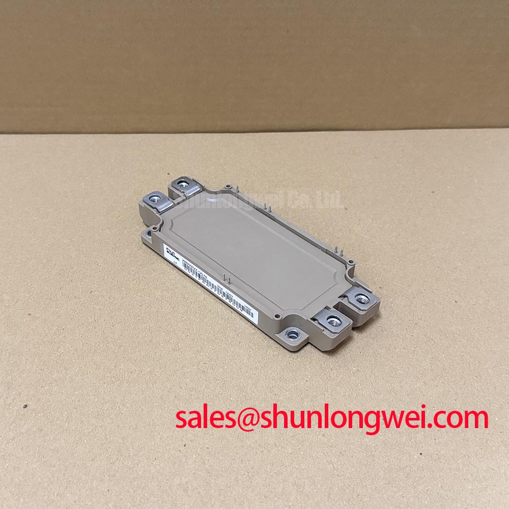
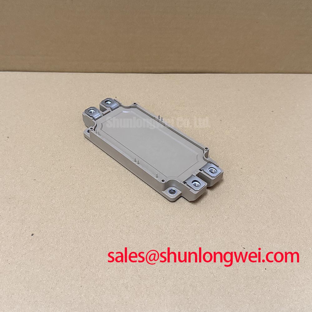
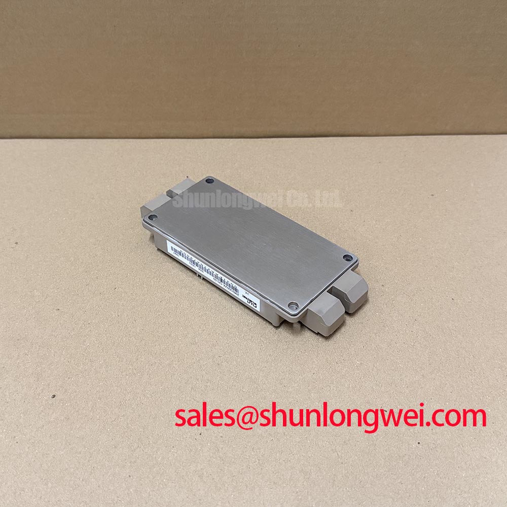
2MBI300VX-120-50 Fuji Electric 1200V 300A IGBT Module
With the DC link fully isolated and discharged, use a digital multimeter in diode-check mode to screen the main power terminals and antiparallel diodes before reconnecting the module to a heavy-duty variable frequency AC motor drive. Keep each gate shorted to its corresponding emitter during main-terminal checks to prevent unintended turn-on from stored gate charge. Record the response in both directions, then inspect the gate terminals for an unintended low-impedance path. This cold-state check does not replace a controlled switching test, but it can prevent a questionable power module from being energized during initial maintenance.
The 2MBI300VX-120-50 is a Fuji Electric power module with a specified voltage rating of 1200.0 V and a rated collector current of 300.0 A under the applicable datasheet conditions. Its listed housing category is Fuji Power Module. These are product identification and rating values for equipment selection; the usable operating point remains dependent on switching frequency, cooling conditions, gate-drive behavior, current waveform, protection coordination, and the complete inverter assembly.
For procurement teams replacing a failed inverter output stage, the mechanical drawing, terminal arrangement, gate-drive polarity, isolation requirements, and heatsink interface should be matched against the removed unit and the original Fuji Electric documentation. A 1200 V, 300 A label alone does not establish interchangeability with another module having a different internal topology, terminal location, thermal interface, or short-circuit capability.
2MBI300VX-120-50 Thermal-Electrical Optimization: Dynamic Gate Impedance Control for Robust Practical Tuning
High dv/dt switching can transfer displacement current through the inactive device gate path and create unwanted turn-on behavior. A practical gate-drive review should therefore begin at the driver output, continue through the gate resistor and return path, and finish at the module terminals. The objective is to keep the commanded gate voltage dominant over parasitic coupling while preserving the switching speed required by the drive’s thermal and efficiency targets.
A low-impedance active Miller clamp is a design consideration when the complementary switch must remain firmly off during the opposing device’s voltage transition. Its effectiveness depends on the physical distance between the driver, clamp path, emitter reference, and module gate terminal. A long shared return trace can add inductive voltage that makes the clamp appear effective in the schematic but weak at the semiconductor terminals. Gate and power commutation loops should be routed separately wherever the mechanical construction permits, with the reference connection taken from the intended emitter or auxiliary emitter point specified by the applicable module documentation.
Negative off-bias can be evaluated as an engineering recommendation when the drive experiences false turn-on during high-voltage transitions. The required value is system-determined and should be selected only after checking the module’s gate-emitter limits, driver isolation, startup behavior, and turn-off transients. The Fuji Electric V-Series IGBT Application Manual provides relevant application guidance for gate control, switching behavior, and protection practices. Designers should verify the actual gate waveform directly at the module terminals rather than relying only on a driver-board test point.
When a drive exhibits irregular current pulses, elevated switching noise, or unexplained heating in one half bridge, compare the high-side and low-side gate-emitter waveforms under the same operating condition. Look for excessive ringing, delayed turn-off, an unstable off-state level, or a difference between the command signal and the voltage measured at the module. The investigation should also include driver power decoupling, isolation capacitance, emitter-reference routing, and the dead-time behavior of the controller. These observations can separate a gate-loop problem from a busbar or load-cable problem without assigning a single cause prematurely.
Long motor cables add another layer of stress. Their distributed impedance and impedance mismatch at the motor can produce reflected voltage waves, creating a motor-terminal peak that differs materially from the bridge waveform. A suitable output filter, cable treatment, or edge-rate strategy is a system-level design consideration. The correct choice should be established from cable length, motor insulation requirements, switching conditions, and measured voltage at both the inverter and motor terminals.
Phase-controlled rectifier front ends can also influence the module’s electrical environment. The rectifier conduction angle affects DC-link ripple and line-current harmonics, while a passive or active harmonic mitigation arrangement changes the ripple current presented to the inverter bridge. When evaluating a replacement module, inspect the DC-link ripple under representative load and confirm that the gate-drive tuning remains stable across the expected rectifier operating range.
2MBI300VX-120-50 Circuit Protection & Reliability: Calibrating Short-Circuit Energy Let-Through Matching
Short-circuit protection must be coordinated as a complete interruption path, not selected from the module’s voltage and current labels alone. The semiconductor fuse, detection circuit, gate shutdown path, DC-link capacitor bank, busbar geometry, and module short-circuit behavior all contribute to the energy delivered before current interruption. Fuse total clearing I²t is relevant to backup protection and any applicable diode surge-withstand assessment, but it does not establish IGBT short-circuit survival. Fast fault detection and gate shutdown must meet the module’s specified short-circuit limits under the applicable conditions.
This coordination is especially important where a fault can be supplied by a charged DC link with low impedance. The protection study should account for fuse operating time, detection delay, gate turn-off behavior, commutation inductance, capacitor discharge contribution, and tolerances in the protection circuit. A fuse that appears suitably fast in a catalog comparison may still fail to protect the IGBT before damage occurs. Delayed gate shutdown increases fault exposure, while fault-loop inductance also affects current rise and turn-off overvoltage.
Busbar construction deserves close inspection after repeated overvoltage events. Laminated positive and negative conductors, short commutation paths, and carefully positioned film capacitors are design considerations for reducing stray inductance and turn-off overshoot. The film capacitor should be placed according to the switching-cell current path rather than simply near the DC-link terminals. Its connection inductance, pulse-current capability, dielectric service conditions, and mechanical support should be checked as part of the assembly review.
The switching overshoot is shaped by the interaction between stray inductance and current change rate. For that reason, the engineering team should measure the collector-emitter waveform with a probe and connection method suitable for fast common-mode transitions. Verify the peak against the DC-link voltage and the applicable module limits during controlled switching tests. A long probe ground lead can create a false ringing signature, while an incorrectly positioned probe can miss the voltage actually present across the module terminals.
Mechanical mounting is equally relevant to protection reliability because poor thermal contact raises junction temperature before an electrical fault occurs. Inspect the flatness of the module-to-heatsink interface, the condition and uniformity of the thermal material, and the mounting hardware. Follow the manufacturer’s mounting sequence and torque instructions so that the module base is not locally distorted.
Maintenance Note: Isolate and discharge the drive before every terminal or gate-cable intervention, then periodically check heatsink cleanliness, thermal-interface aging, airflow, and contact temperature under a repeatable load.
For a cross-reference review, the 2MBI200VB-120-50 may be evaluated as a separate Fuji Electric module option, but it should not be treated as a direct substitute without confirming voltage, current, topology, mounting geometry, terminal assignment, thermal performance, and protection data. The comparison below keeps the verified information distinct from values that require the applicable product documentation.
| Evaluation item | 2MBI300VX-120-50 | 2MBI200VB-120-50 |
|---|---|---|
| Manufacturer | Fuji Electric | Fuji Electric |
| Specified voltage rating | 1200.0 V | Consult applicable datasheet |
| Rated collector current | 300.0 A under applicable datasheet conditions | Consult applicable datasheet |
| Housing category | Fuji Power Module | Consult applicable product documentation |
| Replacement assessment | Reference unit for matching | Engineering compatibility review required |
The comparison is useful during a shutdown because it prevents a lower-current or differently configured device from entering the purchasing workflow solely because the package appears similar. The final selection should follow the original inverter schematic, mechanical drawing, gate-drive design, and measured thermal requirements.
2MBI300VX-120-50 Operational Boundaries: Evaluating Cold-State Main Terminal Impedance Limits
Cold-state screening should be performed with the module disconnected from the DC link, gate driver, motor cable, braking circuit, and any parallel semiconductor path. Keep each gate shorted to its corresponding emitter during main-terminal checks. Use diode-check mode across the main terminals in the expected conduction directions, then reverse the leads and observe whether the response is consistent with the module’s internal power path. The meter reading is a screening observation rather than a universal pass or fail threshold, because instrument current and internal topology affect the displayed value.
Remove the temporary gate-emitter shorts before testing the gate-emitter paths separately, with the gate driver disconnected. An unexpected low-impedance path or a reading that differs markedly between comparable terminals warrants a second measurement. A handheld meter can screen for gross gate damage but cannot establish gate leakage compliance at the specified test voltage. Check the driver board, gate resistor, clamp circuit, and snubber network individually before assigning the result to the power module.
Cold checks should be followed by a visual and mechanical inspection of the terminal hardware. Look for discoloration, loosened fasteners, damaged insulating washers, uneven pressure marks, contamination around the gate terminals, and signs that the heatsink interface has shifted. A clean electrical reading cannot compensate for a poor thermal interface or a loose high-current connection.
During reassembly, confirm the polarity and location of every gate and emitter connection against the original equipment drawing. Keep power-terminal torque and clamping practice aligned with the module manufacturer’s mechanical instructions. The power path should have low-resistance contact across the intended surfaces, while the gate-return path should avoid carrying high-current commutation noise.
Before applying full DC-link voltage, use a staged commissioning procedure with current-limited auxiliary power where the equipment architecture allows it. Confirm gate command timing, interlock behavior, driver supply stability, and the absence of simultaneous conduction commands. Initial energization should be performed with appropriate isolation, controlled load conditions, and waveform monitoring at the bridge terminals.
For maintenance teams supporting industrial variable frequency AC motor drives, the Evolution of Negative Off-Bias Gate Drive Circuits offers a useful engineering reference when evaluating off-state gate control. The design review should include startup and shutdown transitions, fault reset behavior, loss of driver supply, and the interaction between active clamping and negative off-bias. Any chosen gate strategy must remain within the module’s specified gate-emitter limits and be verified under the actual bus voltage, motor cable, load, and cooling conditions.
The 2MBI300VX-120-50 remains a 1200.0 V, 300.0 A Fuji Electric power module reference for replacement assessment. Its integration decision should be supported by terminal measurements, thermal-contact checks, switching waveform evidence, and protection coordination across the complete drive rather than by nameplate comparison alone.