Content last revised on September 10, 2026
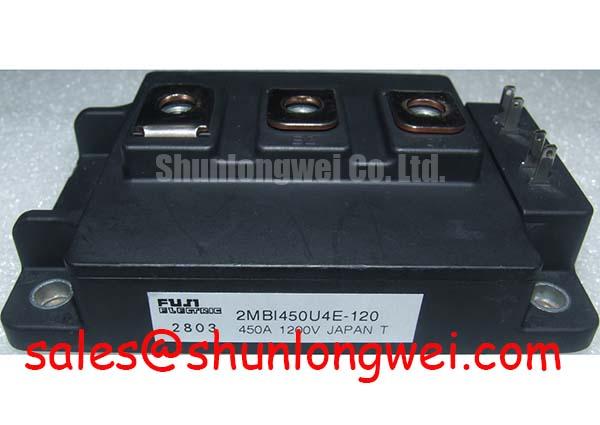
Assembly Integrity & Layout Architecture: Implementing Differential Gate Source Loop Routing to S for 2MBI450U4E-120
Gate loop routing deserves attention before changing gate resistors or protection thresholds. The high current emitter return carries load current and its associated inductive voltage. If that return is shared with the gate driver reference, the driver can interpret power loop noise as a changing gate source voltage. This condition can contribute to unstable switching, false protection events, uneven parallel current sharing, or a gate waveform that differs substantially from the command generated by the controller.
Design Consideration: route the gate drive return through the module’s auxiliary source reference where the module connection arrangement supports it, while keeping the main emitter power path dedicated to load current. The gate and source conductors should be routed as a closely coupled pair, separated from the high current collector and emitter buswork, and kept free of unnecessary connector transitions. The objective is to reduce mutual coupling between the switching current loop and the control loop so the voltage observed at the gate is closer to the voltage intended by the driver.
During a field repair, inspect for lifted small signal terminals, stressed gate leads, conductive debris around the driver board, and return conductors that were moved during a previous service event. A differential probe measurement from gate to the intended source reference is more useful than a ground referenced probe connected at an arbitrary chassis point. Ringing seen only with a long probe ground lead may be a measurement artifact, so confirm the probing arrangement against a known good signal path before modifying hardware.
For topology comparison, the 6MBI450U-120A-05 can be reviewed as a related Fuji Electric module reference, but enclosure geometry, terminal arrangement, circuit topology, drive connections, and thermal interface requirements must be verified against the original equipment documentation. Matching a voltage class alone does not establish installation compatibility.
⚡ Field Alert: Isolate stored energy and confirm the DC link is discharged before connecting, removing, or probing any gate drive cable.
2MBI450U4E-120 Thermal Electrical Optimization: Dynamic Gate Impedance Control for Robust Practical Tuning
A gate driver that turns the device on cleanly in an unloaded test can behave differently when the inverter is connected to its real DC bus and inductive load. The collector voltage transition couples through the IGBT’s internal capacitances into the gate circuit. Where the off state gate path has excessive impedance, this Miller related current can raise gate voltage and create unwanted conduction. In bridge circuits, the resulting cross conduction risk must be evaluated with measured gate source voltage and collector emitter switching waveforms.
Design Consideration: use a driver with a low impedance turn off path and evaluate an active Miller clamp where the gate driver architecture supports it. A negative off state gate bias can improve immunity to induced gate voltage, but the selected value must remain within the official ±20 V VGES rating after cable inductance, ringing, and driver tolerance are included. The required negative bias, source current, sink current, and external gate resistance are system determined and should be confirmed during switching tests.
External gate damping is a balancing exercise rather than a fixed module setting. Lower impedance generally increases switching speed but can make ringing and transient overvoltage harder to control. Higher impedance can suppress oscillation but may increase switching loss or affect protection timing. Engineering Recommendation: adjust the gate network only after observing the real gate source trace, collector emitter voltage, and load current together. Verify the peak voltage margin against the DC link voltage during turn on and turn off tests.
The supplied fault handling context shows why controlled turn off matters. Standard hard turn off can produce peak turn off current slew rates above 5.0 kA/µs, while a two stage soft turn off approach is stated at 1.2 to 2.0 kA/µs. On an 800 V DC rail, the supplied data associates this controlled decay with limiting turn off overshoot to approximately 950 V, instead of an excursion exceeding the 1200 V VCES limit. This is an application level fault response reference and requires confirmation in the completed power assembly.
Fuji Electric’s Brake Chopper IGBT Modules information provides useful context for evaluating switching module roles in energy handling circuits. It should not be treated as a substitute for the specific wiring, protection, and thermal validation required by the installed 2MBI450U4E-120 circuit.
2MBI450U4E-120 Operational Boundaries: Evaluating Optimizing Heatsink Contact Pressure and S Limits
Before mounting the module, clean the heatsink contact area and inspect it under direct light for burrs, corrosion, embedded particles, or local damage left by the removed assembly. These conditions can create localized pressure points or thermal interface voids. A flat, clean mating surface and an evenly spread thermal interface material are essential for transferring heat from the module baseplate to the heatsink.
Design Consideration: thermal interface material thickness should be controlled to fill surface irregularities without creating an unnecessarily thick insulating layer. A common assembly reference range is 50 to 100 µm, but the final material, application method, and thickness must follow the equipment assembly requirement. Where the heatsink surface has measurable curvature, the service team should evaluate whether the interface material and mounting sequence provide uniform contact rather than assuming that higher screw force will correct a mechanical mismatch.
Tighten mounting hardware in a gradual cross pattern so contact pressure develops evenly across the baseplate. The specified torque must be taken from the applicable module mechanical documentation and the equipment’s fastener specification; it is not established here as an official value for this product. After controlled run testing, check for displaced interface material, loosening hardware, abnormal heatsink temperature distribution, or evidence that one area of the contact plane is carrying less load than the rest.
The stated 10 µs SCSOA limit concerns short circuit survivability during fault response and does not replace thermal design verification. Short overload pulses, repetitive switching losses, heatsink performance, ambient condition, and cooling path all affect junction temperature behavior. Engineering Recommendation: assess transient thermal behavior using the original system’s duty cycle and measured case or heatsink conditions, then verify that the protection system clears abnormal current without relying on estimated thermal margins.
A utility scale photovoltaic installation using a 1500 V central inverter architecture requires particular care in defining where this module is used. The official 1200 V VCES rating does not support direct connection across a 1500 V DC bus. Engineers may evaluate the module only for a separately defined lower voltage subsystem where measured steady state and transient conditions remain within the module’s official ratings.
2MBI450U4E-120 Thermal Electrical Optimization: Fault Clearing Dynamics: Type I and Type II Desatur Practical Tuning
Fault response should be checked as a complete chain: current sensing or desaturation detection, controller decision, isolated driver action, IGBT turn off behavior, DC bus transient, and reset logic. A desaturation circuit can respond to an abnormal collector emitter voltage rise, but its blanking arrangement, noise immunity, sensing path, and threshold must be validated for the actual switching waveform. Type I and Type II desaturation approaches can differ in how they coordinate recognition and shutdown, so a circuit copied from another inverter should not be assumed suitable without test evidence.
The supplied module context identifies a standard hard turn off clearing time below 3.0 µs and a two stage soft turn off clearing time of 4.5 to 6.5 µs. It also states that the controlled approach remains within the 10 µs SCSOA limit while reducing gate stress and turn off voltage overshoot. The engineering objective is to prevent a fault shutdown from exchanging excessive current slew rate for excessive collector emitter voltage. The exact handover between the fast and controlled portions of shutdown must be selected and verified by the protection designer.
During commissioning, capture the gate source voltage, collector emitter voltage, fault signal, and DC link behavior with time correlated instrumentation. Check whether the driver remains powered long enough to execute its intended shutdown sequence and whether the protection circuit resets only after the energy storage elements and control logic are in a safe state. If a waveform changes after cable replacement, busbar work, or driver board service, inspect layout and connection integrity before assigning the issue to the module.
Fuji Electric’s RC IGBT Modules resource offers broader device family context for power conversion engineers evaluating integrated switching functions. For system level methods covering device selection, protection coordination, and reliability validation, consult the Power Electronics Masterclass.