Content last revised on October 5, 2026
Field Diagnostics and Commissioning: Voltage Margin and Site Conditions
| Hardware specification | Official Specification |
|---|---|
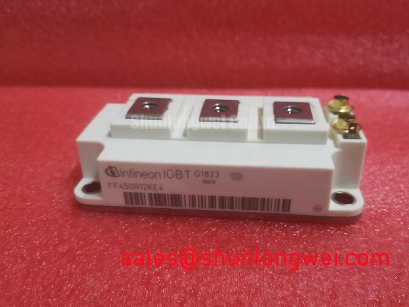
| Model and manufacturer | FF450R12ME3, Infineon |
| Product category and package | IGBT module, module package |
| Rated voltage | 1200 V |
| Rated current | 450 A |
Measure the DC link at the module terminals and capture collector voltage during turn off before approving an FF450R12ME3 installation. Its 1200 V voltage rating is an Official Specification, not permission to operate on every bus described as a 1500 V solar system. A utility scale central photovoltaic inverter is a possible equipment context for evaluation, but its converter topology must establish the voltage actually applied across each module. Compare the measured steady voltage and switching peaks with the module rating under the equipment’s operating conditions.
On a unit returning from service, inspect the terminal area, gate wiring and heatsink contact before interpreting electrical measurements. With the equipment isolated and its DC link discharged, compare cold terminal measurements with a known good assembly using the same meter method. A discrepancy is a reason to investigate the surrounding circuit as well as the module; a single resistance reading does not identify a failure mechanism. During controlled commissioning, correlate gate commands, DC link voltage and collector voltage on the same switching event. That record is more useful than attributing a trip to the module from an alarm code alone.
Altitude and terrestrial neutron exposure can matter to high voltage semiconductor reliability, but an installation altitude does not establish a device specific single event burnout rate. Design Consideration: If the site’s reliability assessment requires a failures in time estimate, obtain applicable manufacturer reliability data and the equipment’s voltage and environmental profile before calculating one. Neither a FIT figure nor an altitude derating value can be inferred from the 1200 V rating. Infineon’s IGBT modules and discretes portfolio provides manufacturer context for reviewing device documentation; The Ultimate IGBT Knowledge Base provides background on switching and failure mechanisms without replacing a model specific reliability assessment.
FF450R12ME3 Operational Boundaries: Evaluating an Active Miller Clamp
Probe gate to emitter voltage at the module connection while the opposing switch changes state. A gate disturbance coincident with that transition warrants investigation of gate loop impedance, driver return routing and any active Miller clamp in the existing driver. Do not diagnose cross conduction from a gate trace alone: compare it with the collector voltage, current waveform and driver fault record under a controlled test.
An active Miller clamp can provide a low impedance path that restrains unwanted gate voltage rise during a rapid collector voltage transition. Design Consideration: Its usefulness depends on where the clamp senses the gate, how it connects to the emitter return and whether it operates through the relevant switching interval. The driver design determines gate bias and clamp implementation; the supplied specifications do not establish a negative bias requirement or a permissible value for this module. Verify gate limits and operating conditions in the applicable Infineon documentation before changing an installed driver.
Inspect the protection sequence alongside the clamp circuit. If desaturation protection is fitted, capture when the driver asserts a fault relative to the gate command and when collector voltage begins to recover. The detection threshold, blanking interval and turn off behavior belong to the driver and system design. Assigning a universal detection time to FF450R12ME3 from its voltage and current ratings would conceal differences in wiring, noise and fault current paths.
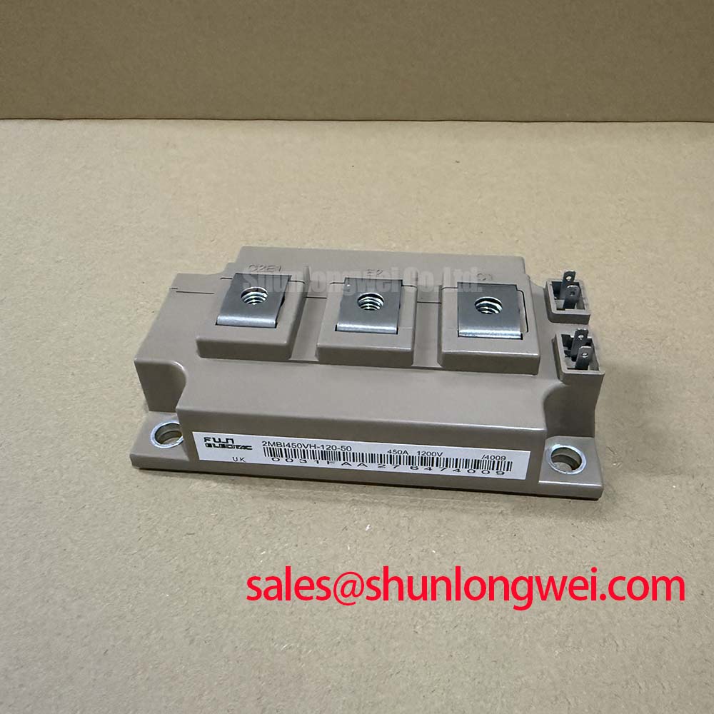
Replacement comparisons need the same discipline. FZ800R12KS4_B2 is a separate model to assess against the original circuit, not a drop in substitution established by its name or headline ratings. Compare topology, terminal arrangement, mounting interface, driver requirements and protection behavior against the equipment drawings before considering any change.
Field Diagnostics and Commissioning: DC Link Layout and Switching Overshoot
Capture the voltage peak across the module during a controlled turn off and compare it with the DC link voltage recorded at the same instant. The difference can reflect energy in the commutation loop’s parasitic inductance, although probe placement and bandwidth can distort the apparent peak. Repeat a suspicious measurement with an appropriate high voltage measurement setup and a short, well defined probe connection before changing the snubber or condemning the module.
Engineering Recommendation: Keep the DC link capacitor connection and opposing current paths compact and symmetrical to limit inductive overshoot, then verify the resulting peak voltage under the system’s switching conditions. A laminated busbar or local snubber may be evaluated where the equipment design supports it, but neither a busbar inductance target nor a snubber value follows from the module’s 1200 V and 450 A Official Specifications. The system engineer must evaluate voltage margin, capacitor ripple duty and switching loss together.
For a persistent peak, inspect capacitor terminations, busbar joints and the return path for looseness, contamination or evidence of heating. Compare waveforms before and after any approved repair at the same operating point. Keep the maintenance record tied to measured conditions: a lower peak after tightening a connection supports further investigation of that joint, but does not by itself prove that the joint was the only cause of an earlier trip.
Maintenance Note: Isolate and discharge the DC link before touching busbar joints, and check contact temperature and heatsink airflow during scheduled maintenance. Dust buildup can restrict cooling, while changes at thermal interfaces or power terminals may alter operating temperature. Inspect those interfaces under the equipment’s maintenance procedure rather than imposing an unverified service interval for the module.
FF450R12ME3 Circuit Protection and Reliability: Calibrating Desaturation Detection
Capture the fault input, gate waveform and collector voltage during a controlled protection test, then check whether the driver recognizes the intended fault without responding to ordinary switching transients. Desaturation detection relies on the relationship between collector voltage and commanded conduction; its threshold and blanking behavior must be coordinated with the driver circuit and switching noise. A trip during normal commutation may call for signal path inspection, not an immediate increase in the threshold.
Design Consideration: A staged or soft turn off can reduce the abrupt current change that contributes to inductive overvoltage during a fault. Its timing and gate trajectory remain system determined. Verify the fault response against the applicable module short circuit operating limits and the equipment’s measured voltage peak; the supplied Official Specifications do not establish a model specific short circuit duration or mandate a particular protection sequence.
Check the complete protection path after service: gate driver supply, fault wiring, current sensing where fitted, and the controller’s response to the driver fault signal. Record the tested operating point and waveforms so the next maintenance team can distinguish a changed fault response from a changed load condition. For an FF450R12ME3 in a central solar inverter assessment, that record should also identify the voltage across the individual module. The inverter’s nominal system voltage cannot stand in for that measurement.