


Content last revised on September 14, 2026
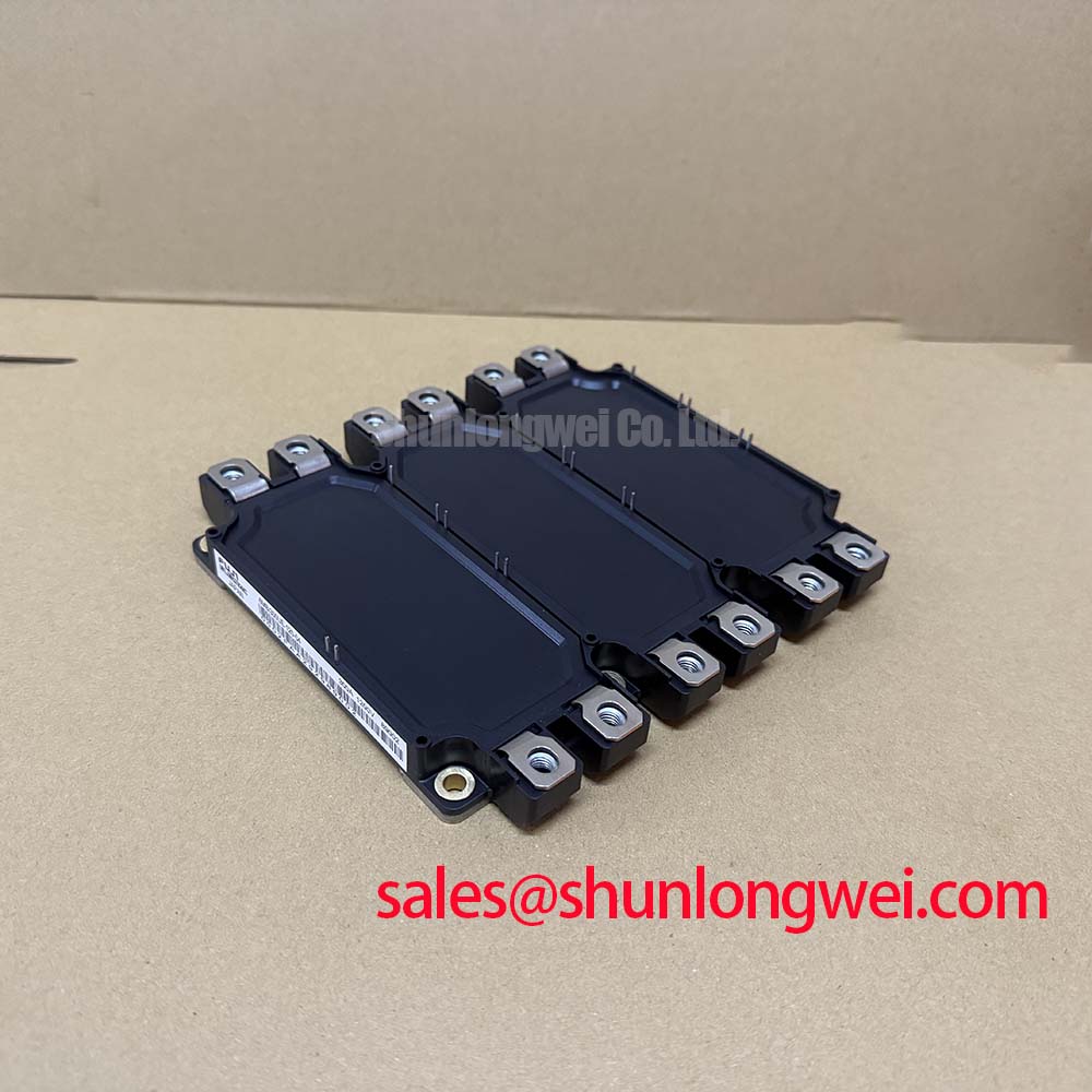
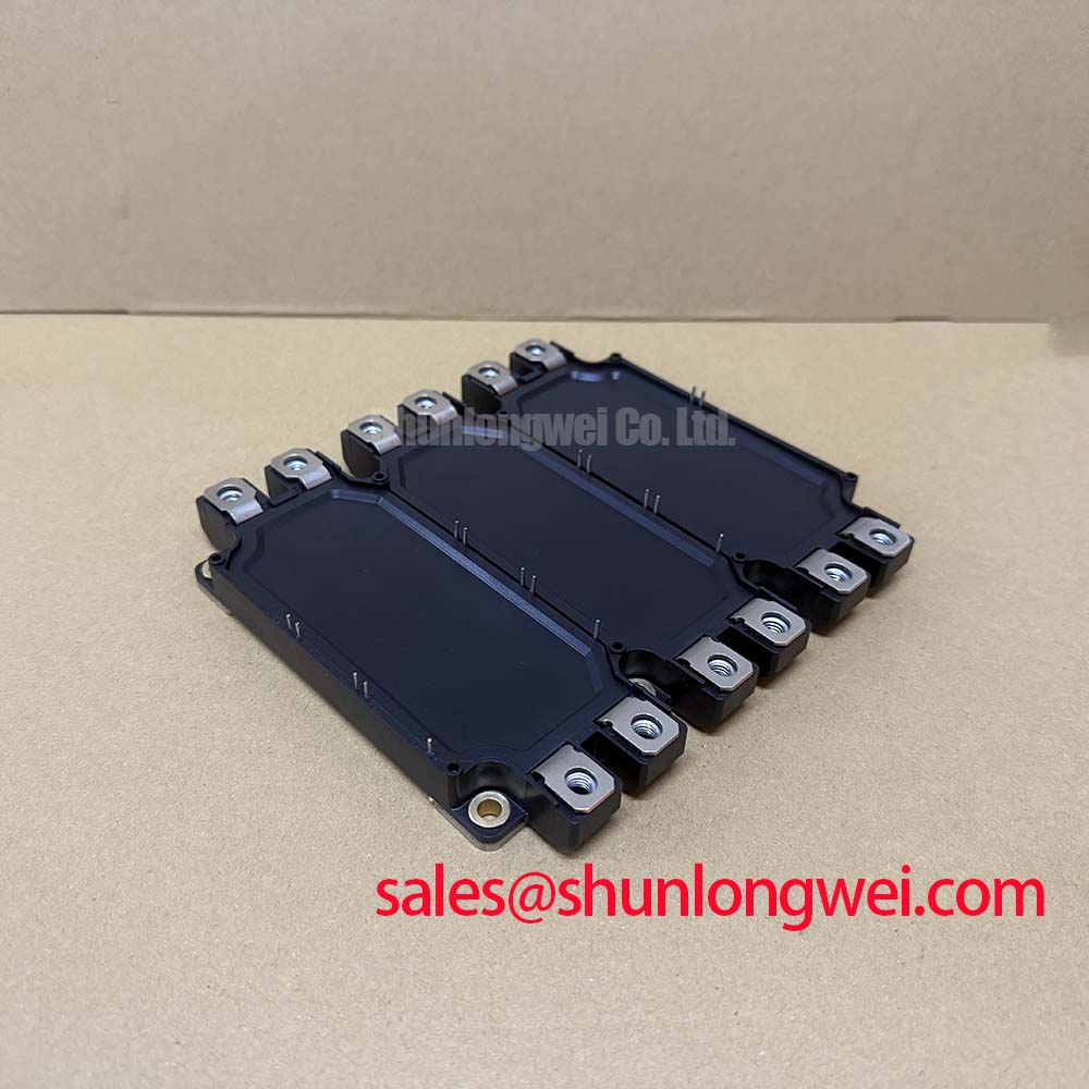
6MBI300UE-120-04 Thermal-Electrical Optimization: Cosmic Ray Robustness, Voltage Derating and Practical Tuning
The module combines a high voltage rating with a low conduction and switching loss balance. Fuji Electric specifies VCE(sat) at 1.8 V typical and 2.3 V maximum, with the typical value also stated at 25°C. The specified typical turn-off energy is Eoff = 28 mJ per pulse, while total typical switching energy is listed as Ets = 50 mJ. These values help engineers compare conduction and switching behavior, but they do not by themselves define the allowable PWM frequency or the complete thermal limit of a commercial string inverter.
For a 400 V to 575 V AC inverter front end, designers should verify the actual DC-link voltage, regeneration overshoot, braking events, and switching-node ringing rather than relying on nominal line voltage alone. The 1200 V VCES rating provides a substantial voltage boundary, but the usable operating margin remains system dependent. During commissioning, capture the collector-emitter waveform at the module terminals with suitable high-voltage probing and compare the peak value with the DC-link operating range under acceleration, deceleration, grid disturbance, and energy-storage transitions.
Cosmic-ray and terrestrial-neutron discussions require a qualified device-specific reliability source before any FIT, SEB probability, altitude limit, or lifetime number is assigned. No such numerical field or reliability data should be inferred from the voltage rating alone. At elevations above 2000 m, atmospheric and cooling conditions can change at the same time as electrical stress. A suitable Design Consideration is to review DC-link headroom, insulation coordination, enclosure cooling, creepage, clearance, and transient suppression as one system assessment. The final voltage derating decision should be validated by the inverter manufacturer using measured switching peaks and the applicable qualification documentation.
Thermal inspection should start at the baseplate and heatsink interface. The stated junction-to-case thermal resistance is Rth(j-c) = 0.08 K/W per IGBT, an official specification value that supports heatsink calculations when used with the complete thermal network. It does not represent the full case-to-heatsink or heatsink-to-ambient path. For pulsed operation, engineers should evaluate transient thermal impedance, pulse duration, duty cycle, and adjacent-chip heating before accepting a peak current or short overload.
In a braking chopper or regenerative path, the resistor and switching device must be evaluated together. The operating principle described in dynamic braking references can assist with topology review, while current feedback may be assessed using industrial transducers such as those described by LEM current sensors. These external references explain system functions; they do not extend the Fuji module’s official ratings.
Field Diagnostics and Commissioning: Galvanic Gate Drive Isolation in 6MBI300UE-120-04 Topologies
Before connecting the isolated gate driver, identify every power, gate, emitter, and auxiliary terminal from the original Fuji Electric documentation. A resistance check between control-side and power-side conductors can reveal an unexpected connection, but a multimeter result is not an insulation qualification test. Reinforced isolation, dielectric withstand, and common-mode transient immunity belong to the complete driver, isolation barrier, PCB, connector, and power stage. If a design requires more than 5 kV isolation or CMTI above 100 kV/µs, the system integrator must verify those values from the selected driver and safety documentation rather than attributing them to the IGBT module.
A practical incoming test uses a calibrated meter in diode mode to compare the freewheel diode path with a known-good reference unit of the same documented configuration. Keep the module unpowered, use ESD controls, and record probe polarity, ambient temperature, and lead placement. A different reading may indicate a measurement-path issue, parallel circuitry, contamination, or device damage; it should be investigated with isolation from the surrounding circuit and, where necessary, a curve tracer or approved semiconductor tester.
Gate-emitter checks should remain within the test equipment’s safe low-energy limits. Do not apply an arbitrary gate voltage merely to obtain a switching result. Confirm the required gate supply, gate resistance, UVLO behavior, interlock logic, and dead-time from the driver design documentation. When the power stage uses a related front-end or complementary topology, the 2MBI300U4H-120-50 may be reviewed as a separate system-level reference, but compatibility must be established from terminal definitions and electrical ratings.
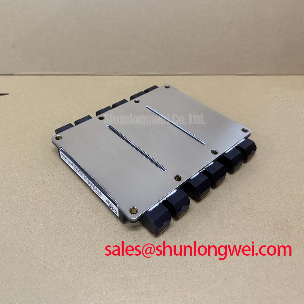
The thermal interface is part of the commissioning procedure, not an afterthought. The heatsink surface should be clean, flat, and free of particles. A thin, uniform TIM layer is a common Design Consideration; the specified application thickness must come from the TIM supplier and heatsink assembly procedure. For mounting, use a gradual cross-pattern tightening sequence and the approved fastener torque from the module or equipment service documentation. Bench Tip: keep the module isolated from the DC link and protect the gate terminals from ESD while making every cold-state comparison.
After installation, inspect the thermal interface imprint and verify that the baseplate is seated evenly. A hot spot may result from uneven pressure, poor TIM distribution, blocked airflow, excessive switching loss, or an abnormal current path. Use thermocouples or infrared measurement with known emissivity limits, then correlate case temperature with gate waveform, collector current, and switching timing.
6MBI300UE-120-04 Thermal-Electrical Optimization: High-Speed Fault Management and VCE Desaturation Tuning
The specified short-circuit withstand time is tsc ≥ 10 µs. This is an official module specification and should be treated as a maximum protection response boundary, not as permission to operate repeatedly in a short-circuit condition. Desaturation protection, current sensing, blanking behavior, gate shutdown, and fault latching are functions of the complete gate-driver and control system.
For a type I or type II short-circuit response, the protection chain should detect abnormal collector-emitter behavior promptly, control the gate current during shutdown, and prevent a second turn-on command until the fault state is understood. A two-stage soft turn-off strategy can be considered when testing shows that an abrupt gate discharge creates excessive inductive overshoot. The correct timing and damping values are system determined and require oscilloscope verification at the module terminals.
During fault testing, monitor VCE, gate-emitter voltage, collector current, driver supply behavior, and the fault feedback signal on the same time base. A failed test may involve desaturation threshold selection, an unsuitable blanking interval, current-sensor delay, gate-loop inductance, driver saturation, or DC-link layout. Avoid assigning one cause from the symptom alone. Compare the waveform with the known-good phase leg and inspect the complete protection path.
Short-circuit coordination also involves the upstream semiconductor fuse. The fuse’s I²t characteristic, clearing behavior, wiring inductance, and module short-circuit capability must be reviewed together. A fuse cannot be assumed to protect the IGBT during every fast internal fault because the semiconductor may experience damaging electrical stress before the fuse clears. The equipment designer should validate the coordination through the relevant manufacturer data and controlled fault testing.
Long motor cables and inverter output filters can create reflected-wave stress at the motor terminals and additional switching-node ringing at the power module. Filter selection, cable impedance, termination, common-mode control, and dv/dt behavior should be evaluated from measured waveforms. Do not assign a fixed “safe” cable length or filter value to this module without the motor, cable, inverter, and installation data.
Preventing Spurious Faults: PCB Symmetry Considerations for Dual IGBT Guidelines for 6MBI300UE-120-04
Keep the high-current commutation path physically short and separate from the gate-driver return path. Where the package provides an auxiliary emitter connection, route that control reference independently from the main emitter current path when the terminal documentation supports that arrangement. Shared copper can introduce voltage displacement during rapid current change, which may appear as gate bounce, false desaturation, uneven switching, or oscillation.
For a dual-IGBT phase leg, match the gate-loop geometry, resistor arrangement, driver placement, and return routing between the two switching positions. Symmetry does not mean copying a layout without checking the actual current direction and commutation loop. The designer should minimize parasitic inductance in the gate and power loops, then verify turn-on and turn-off waveforms under the highest intended current and switching stress.
Inspect the PCB for solder voids, lifted terminals, cracked joints, contamination, and unintended copper bridges before energizing the module. Confirm that control isolation is maintained across the board and that the gate driver cannot issue simultaneous commands to opposing devices. Dead-time and interlock values must be selected from the switching behavior of the complete inverter, with microsecond-scale timing validated on the bench rather than copied from an unrelated module.
When a replacement assessment is required, the 6MBI300U-120 can be examined as a same-family reference, but terminal arrangement, switching characteristics, thermal interface, and protection settings must be checked before any interchange decision. For engineers comparing silicon IGBT behavior with newer power technologies in high-stress converter positions, the Wide Bandgap Revolution article provides broader technology context without replacing the Fuji Electric documentation for this module.
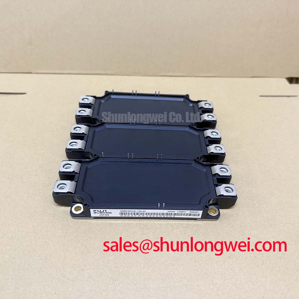
For commercial string inverters and micro-grid energy-storage converters, final acceptance should combine cold-state terminal records, isolation checks, gate-waveform inspection, thermal measurements, fault-interlock verification, and controlled load testing. The 6MBI300UE-120-04 provides a documented 1200 V, 300 A class platform with typical low-loss values, while safe integration remains dependent on the surrounding driver, protection, cooling, busbar, cable, and control design.