

Content last revised on September 10, 2026
FZ800R12KS4_B2 Operational Boundaries: Evaluating Kelvin Emitter Connection Limits
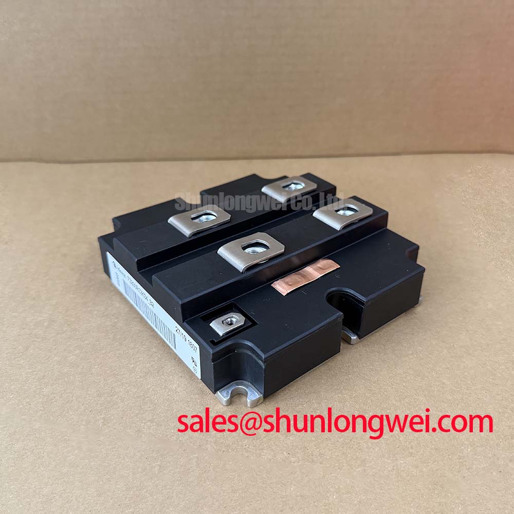
Before energizing a test fixture, isolate the FZ800R12KS4_B2, confirm the marked collector, emitter, gate, and auxiliary connections against the original circuit documentation, then record a cold-state diode-mode baseline with an ESD-safe meter.
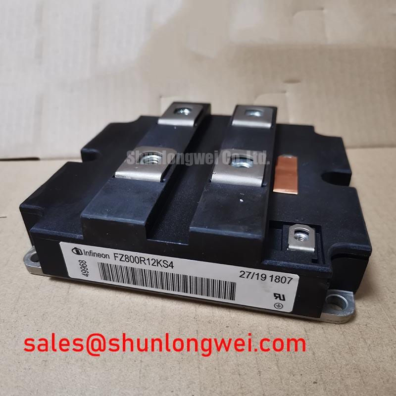
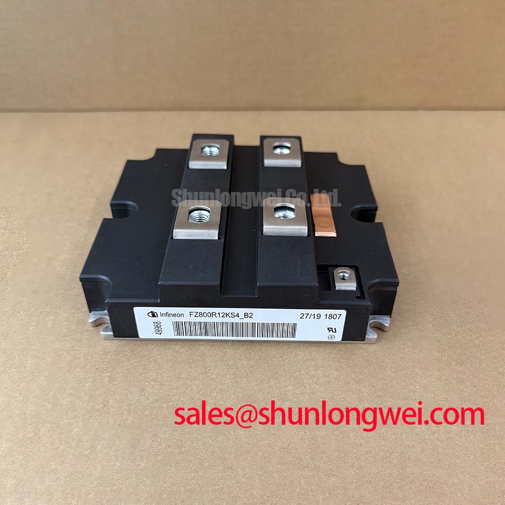
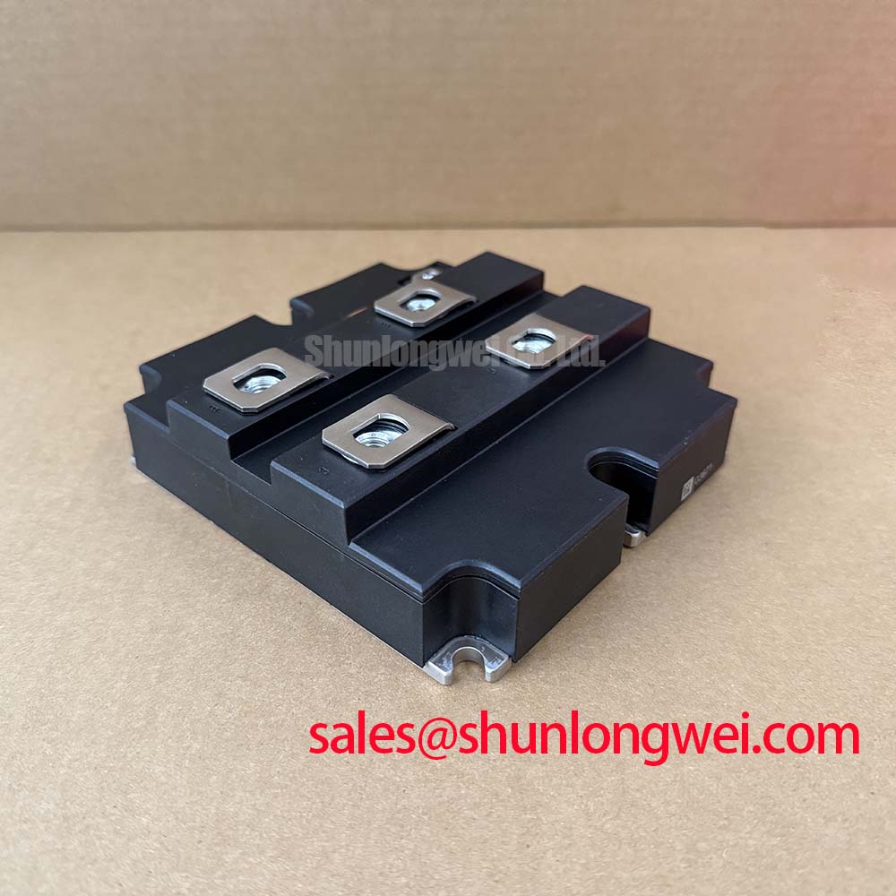
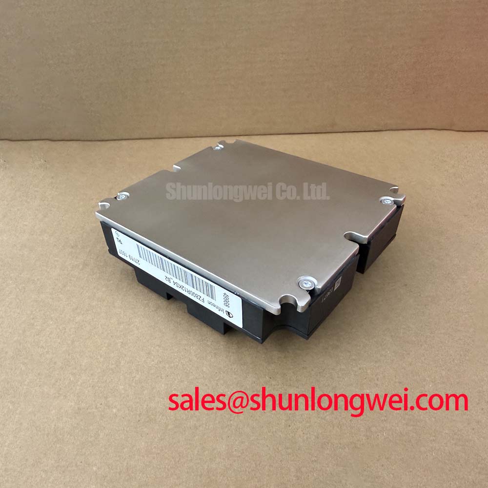
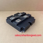
The Infineon FZ800R12KS4_B2 is a high-current IGBT module specified for power conversion systems that require a 1200 V collector-emitter voltage class and a continuous DC collector current of 800 A under the stated case-temperature condition. Its published electrical limits should be read together with switching energy, thermal resistance, gate insulation, cooling interface, and protection design. For a utility-scale centralized battery energy storage PCS, the device may be evaluated in a bidirectional inverter bridge, subject to the complete topology, cooling system, gate driver, protection coordination, and applicable system validation.
| Parameter | Official specification | Test condition |
|---|---|---|
| Collector-emitter voltage | VCES 1200 V | Tvj = 25°C |
| Continuous DC collector current | IC nom 800 A | TC = 80°C |
| Repetitive peak collector current | ICRM 1600 A | tp = 1 ms |
| Total power dissipation | Ptot 7600 W per IGBT | TC = 25°C |
| Repetitive peak reverse voltage | VRRM 1200 V | Tvj = 25°C |
| Collector-emitter saturation voltage | 3.20 V typical, 3.70 V maximum | IC = 800 A, VGE = 15 V, Tvj = 125°C |
| Gate-emitter leakage current | IGES 400 nA | VCE = 0 V, VGE = 20 V, Tvj = 25°C |
| Turn-on energy loss | Eon 760 mJ per pulse | IC = 800 A, VCE = 600 V, Tvj = 125°C |
| Turn-off energy loss | Eoff 580 mJ per pulse | IC = 800 A, VCE = 600 V, Tvj = 125°C |
| Junction-to-case thermal resistance | RthJC 16.5 K/kW | Per IGBT |
| Case-to-heatsink thermal resistance | RthCH 13.5 K/kW | Per IGBT with paste |
The first layout question is whether the gate-drive return is separated from the high-current emitter path in the actual module connection scheme. The supplied parameter set does not by itself confirm a specific auxiliary Kelvin emitter arrangement, so the system integrator should verify the terminal drawing and original Infineon documentation before assigning any pin as a Kelvin reference. If the module provides a dedicated low-current emitter sense connection, route it directly to the gate driver return and keep it separate from the power emitter conductor until the intended reference point.
This separation is a Design Consideration, not an additional factory rating. When collector current changes rapidly, shared copper, busbar joints, bolts, and flexible links can develop voltage differences that appear at the gate loop. The driver may then see an unintended gate-emitter voltage, creating ringing, delayed turn-off, or unequal switching between parallel positions. The practical objective is to minimize mutual coupling and parasitic loop inductance while allowing the power path to carry the specified current without forcing its return current through the signal reference.
During incoming inspection, compare the terminal marking, baseplate condition, insulation interfaces, and mechanical drawing with the removed unit. A diode-mode check can help establish the polarity of the internal freewheel path, but it is not a substitute for a controlled semiconductor curve tracer or the manufacturer’s test method. Measure with the module fully isolated from the driver, discharge any external capacitors, and record the meter polarity, lead arrangement, and ambient condition. A materially different cold-state reading from a known-good reference may justify further testing; it should not be treated as proof of one particular failure mechanism.
For a battery PCS, review the gate-return route across every commutation cell, including laminated busbars, current sensors, contactor interfaces, and service disconnect wiring. The gate loop should not run alongside a high di/dt power path for a long parallel distance. Keep the driver reference physically tied to its intended emitter reference, reduce unnecessary loop area, and use a controlled shield or grounded reference strategy where the enclosure and isolation architecture permit it. Designers should verify gate voltage and collector-emitter overshoot with a properly rated differential probe during turn-on, turn-off, regenerative operation, and abnormal-load testing.
When comparing system documentation, the FZ3600R12HP4 can be reviewed as a neutral same-family reference, but its electrical, mechanical, and gate-drive details must not be transferred to this device without direct documentation and fit verification.
Preventing Spurious Faults: DC-DC Converter Interleaving and Ripple Cu Guidelines for FZ800R12KS4_B2
A bidirectional battery PCS changes current direction between battery racks and the inverter link. That four-quadrant power flow places the gate supply, isolation barrier, DC-link capacitors, and protection circuits under alternating operating conditions. A gate driver that appears stable during forward power transfer can show supply ripple or undervoltage behavior during regeneration. Interleaved auxiliary converters can reduce input-current concentration, but their phase relationship, control loop response, transformer leakage, and local decoupling must be verified on the assembled board rather than assumed from the schematic.
The gate supply network should be evaluated at the module connector under the real switching current, not only at the converter output. Use short, low-impedance power and return paths, separate high-current converter loops from sensitive gate-sense traces, and place local bypass components according to the driver manufacturer’s layout guidance. Ripple copper should be sized for its thermal and current-density requirements while avoiding broad copper regions that increase capacitive coupling into isolated control domains.
For a bootstrap-based high-side supply, capacitor selection is an Engineering Recommendation based on the driver’s gate charge demand, quiescent current, switching frequency, permitted supply droop, leakage, temperature, and recharge interval. The required charge must cover the high-side gate charge and all driver-side consumption during the longest high-side on-time, with additional allowance determined by the system designer for component tolerance and ageing. The bootstrap diode must also be checked for reverse-recovery behavior, peak current, blocking voltage, and compatibility with the driver’s switching sequence. A bootstrap arrangement may be unsuitable where the topology cannot provide adequate refresh time.
The official IGES value is 400 nA at VCE = 0 V, VGE = 20 V, and Tvj = 25°C; this is a gate-emitter leakage specification for the module and should not be used as the total gate-driver supply budget. Driver quiescent current, isolation-device consumption, pull-down networks, charging losses, and temperature effects remain system variables. During commissioning, monitor the isolated gate supply at the driver pins with a short probe connection and correlate any fault flag with the gate waveform, DC-link voltage, and current command.
The BSM75GD120DLC may be relevant as a neutral reference when reviewing an associated rectifier or complementary power stage, but it does not establish the electrical compatibility of a driver, converter, or protection network for this module. Engineers should check the complete topology, voltage class, pulse current, isolation arrangement, and mechanical interface independently.
For utility-scale battery equipment, phase-controlled rectification upstream of the DC link can introduce line-current distortion when the conduction interval is narrow. The firing strategy, AC impedance, filter, pulse pattern, and grid-code requirements determine the harmonic result. The IGBT module itself does not guarantee harmonic compliance. Designers should verify power factor, current distortion, and thermal loading at the point of common coupling using the applicable installation standard and the complete converter control scheme.
Benchtop Waveform Tuning: Mitigating Stress via Common-Mode Transient Immunity in Harsh IGBT Switching
Waveform tuning should begin with a safe, isolated measurement arrangement. Confirm probe common-mode ratings, differential probe bandwidth, grounding method, and the isolation boundary before applying a switching command. A gate waveform that looks clean relative to laboratory ground can be misleading if the actual driver reference is moving with the emitter. Measure gate-to-emitter voltage at the module terminals and observe the collector-emitter transition with a suitable high-voltage probe.
Reinforced isolation barriers and high common-mode transient immunity are Design Considerations for this application, not official ratings supplied for the FZ800R12KS4_B2 in the stated parameter list. A system may establish an engineering target above 5 kV insulation withstand and above 100 kV/µs CMTI, but the complete driver, isolator, PCB spacing, coating, connector, transformer, and enclosure must be qualified together. These values must not be presented as guaranteed characteristics of the IGBT module.
Maintain the isolation distance required by the applicable safety standard and pollution environment, with creepage, clearance, material group, altitude, and working-voltage conditions determined by the system safety assessment. Keep high dv/dt copper away from isolated logic traces, avoid unnecessary capacitive bridges across the barrier, and provide a deliberate return path for displacement current. The final design should be tested with the actual DC-link voltage, switching speed, cable arrangement, and enclosure geometry.
Spurious gate pulses can also arise from Miller coupling, driver saturation, inadequate gate discharge, probe loading, or a floating reference. If an unexpected pulse is observed, first compare it with a known-good channel using the same probe and measurement position. Then inspect driver supply stability, gate resistance population, emitter-reference continuity, isolation-device output behavior, and turn-off timing. Do not infer module damage from a single oscilloscope trace without checking the complete signal path.
The official switching data provides Eon 760 mJ and Eoff 580 mJ per pulse at IC = 800 A, VCE = 600 V, and Tvj = 125°C. These figures describe specified test conditions, not a universal loss value for every PCS operating point. Switching frequency, current direction, gate resistance, stray inductance, temperature, diode behavior, and modulation strategy all affect actual thermal loading. The Infineon IGBT Modules Overview is a useful manufacturer reference for interpreting module-level application information, while the RCDC application note should only be applied where the topology and device type match its scope.
Field Diagnostics & Commissioning: SCSOA Overcurrent Protection in FZ800R12KS4_B2 Topologies
Overcurrent protection should be commissioned with the gate command disabled, the DC link safely discharged, and the current-sensing chain checked independently. Inspect the sensor polarity, desaturation or collector-voltage sensing path, blanking behavior, isolation feedback, fault latch, and gate-driver supply before applying controlled power. The module’s ICRM rating is 1600 A for a 1 ms pulse; this repetitive peak specification does not define an unlimited short-circuit operating area or authorize a particular protection delay.
A proposed short-circuit detection interval below 10 µs is a system protection target from the application brief and must be validated against the manufacturer’s short-circuit data, gate-driver delay, sensor response, wiring inductance, and actual test waveform. It is not an official FZ800R12KS4_B2 parameter in the supplied table. Designers should obtain the applicable device switching and short-circuit operating-area information before setting type-I or type-II protection behavior.
Two-stage soft turn-off can be considered when a direct gate clamp would create excessive inductive voltage. The first stage limits the rate of current reduction, while the subsequent stage establishes a defined off-state and fault latch. The actual sequence, gate voltage, timing, and fault energy must be determined by the driver and power-loop design. Minimize parasitic inductance in the commutation path and verify the resulting collector-emitter peak against the DC-link voltage during controlled fault tests.
Protection coordination also includes the DC-link clamp and the upstream semiconductor fuse. MOV selection, snubber design, active clamping, and busbar geometry should be treated as a coordinated overvoltage network rather than separate catalogue choices. The MOV must be checked for continuous operating voltage, temporary overvoltage, energy absorption, ageing, and thermal disconnection in the complete installation. A fuse should be selected by comparing its published clearing behavior and I²t with the module’s permitted fault energy and the system’s prospective current; the module rating alone cannot establish fuse suitability.
For a phase-controlled rectifier or active front end, current limiting and harmonic control affect the fault current available to the inverter bridge. Confirm firing-angle behavior, DC-link precharge, contactor sequencing, current-sensor saturation, and battery rack isolation before enabling peak-shaving commands. If several modules are paralleled, positive temperature coefficient behavior may support static sharing, but dynamic sharing still depends on matched gate paths, symmetrical busbar impedance, thermal coupling, switching tolerances, and separate measurement. Designers should validate current balance at startup, rated load, regenerative transfer, and fault recovery.
Record the gate-to-emitter waveform, collector-emitter voltage, phase current, DC-link voltage, driver supply, and fault timing for each commissioning event. Compare the traces with the module’s official conditions rather than treating a field symptom as a single-cause diagnosis. Long-term operating assessments should be linked to documented test methods and system evidence; the Industrial Applications resource can provide broader application context, while final qualification remains the responsibility of the equipment design and verification process.
💡 Bench Tip: Keep the module shorted or safely isolated during cold-state checks, use ESD protection, and compare every diode-mode reading with a documented known-good baseline before applying gate power.