


Content last revised on November 6, 2026
Field Diagnostics and Commissioning for Gate Drive Loop Geometry
Gate drive troubleshooting should begin at the physical return path, not at the driver supply setting. In a high current IGBT stage, the emitter reference used by the gate driver can move during commutation if it shares copper, vias, terminals, or busbar sections with the load current return. That movement appears at the driver as an unwanted gate signal and can promote oscillation, false turn on, or excessive switching loss.
Where the module interface provides an auxiliary emitter or Kelvin style gate return, route that return separately from the main high current emitter path until the intended reference point is reached. The purpose is to reduce mutual coupling between the power loop and the gate loop. The control return should not be allowed to follow a long parallel section of the collector or emitter busbar, and it should not be casually joined to the power return at a distant chassis point.
During a field repair, photograph the original conductor arrangement before removing the failed module. Mark the gate lead, driver return, power emitter, and any shield or auxiliary connection. A replacement wire that is electrically continuous may still be unsuitable if it changes the loop area or introduces a shared inductive section. Keep the outgoing gate path and its return close together, while keeping that pair physically separated from the high current commutation path.
Use an oscilloscope with an appropriate differential or isolated measurement method to examine the gate to emitter voltage at the module terminals rather than only at the driver board. A clean waveform at the driver board does not prove that the voltage at the module gate is clean. Compare turn on and turn off behavior under controlled operating conditions, looking for ringing that follows the power commutation event, unexpected plateau extension, or a gate excursion when the opposite device changes state.
Dead time should be treated as a system timing parameter. The correct interval depends on driver propagation delay, device switching behavior, load current, temperature, DC link conditions, and the measured behavior of the complementary switch. Designers should adjust it only after confirming that the gate signals cannot overlap at the module terminals. A direct driver output test without the module connected can miss parasitic effects introduced by the actual power layout.
Gate loop damping is also layout dependent. A resistor placed at the driver board may not control the same oscillation as a resistor placed close to the module gate terminal. When oscillation is suspected, compare the waveform at both locations and change one variable at a time. The objective is controlled switching with acceptable overshoot and loss, not simply the fastest edge available from the driver.
For an industrial inverter welder or a medium frequency induction heating supply, the service engineer should also inspect the driver isolation barrier, local decoupling, gate clamp path, and connector retention. A loose control connector can produce intermittent gate behavior that resembles a layout problem. Check the gate to emitter path with the power removed, then compare each channel with an equivalent healthy channel while respecting the measurement limits of the test instrument.
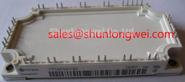
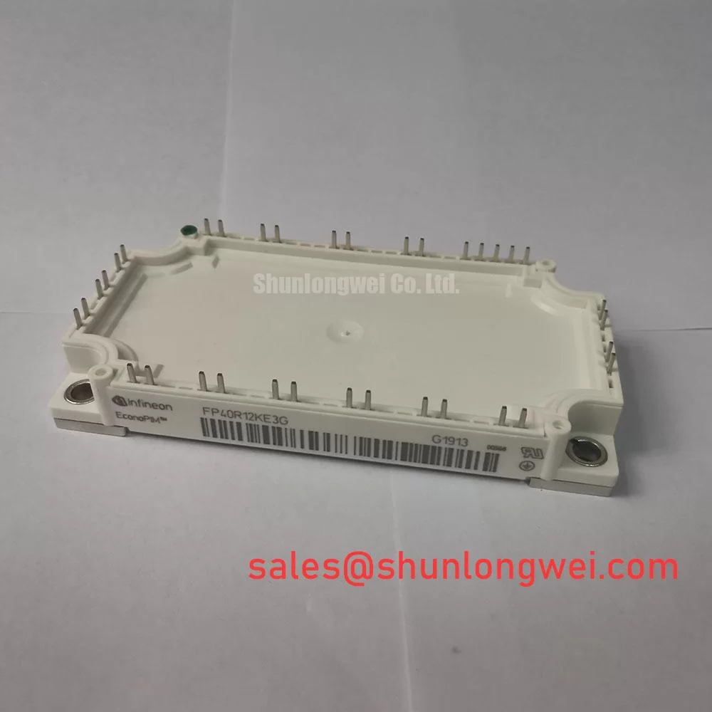
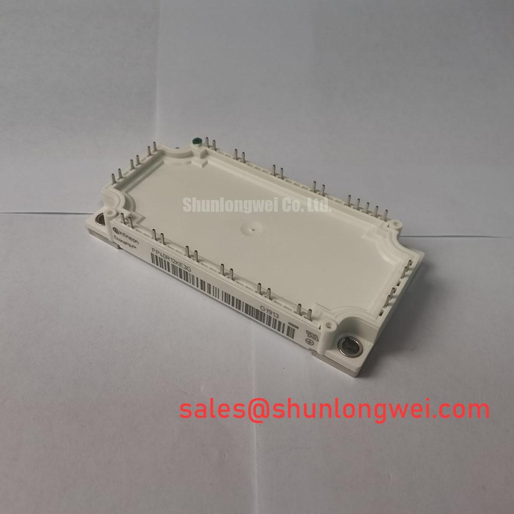
FP40R12KE3G Circuit Protection and Turn Off Transient Control
Turn off protection is governed by the interaction of DC link voltage, commutation current, stray inductance, and switching speed. The transient relationship can be described in the switching loop as Vpeak rising with the product of stray inductance and current change rate, added to the DC link voltage. This relationship is an engineering calculation for the complete power loop, not an additional rating of the FP40R12KE3G.
Start the protection review by identifying the physical commutation loop from the positive bus, through the module, and back to the negative bus. Symmetrical planar busbar construction generally helps reduce loop area and unequal current distribution, but the actual result must be verified at the module terminals. A compact arrangement is useful only when insulation spacing, service access, creepage, and thermal construction remain acceptable.
Measure the turn off collector emitter waveform with a probe arrangement that does not add a large measurement loop. A long ground lead can create an apparent overshoot that is not present in the power circuit, while an unsuitable differential probe can obscure fast ringing. Compare the measured peak with the permitted voltage boundary for the selected operating condition and confirm the result across load current, temperature, and switching states.
Snubber selection should follow the observed transient rather than a generic capacitor value. The capacitor, resistor, or clamp network must absorb the relevant high frequency energy without creating excessive reactive current or additional turn on loss. Designers should evaluate the location of the snubber, its connection inductance, pulse current capability, dielectric behavior, and thermal dissipation as one network. A snubber mounted far from the module may provide little benefit against the first voltage spike.
Active gate control can complement the power loop design when the driver supports it. Miller plateau behavior, reverse transfer capacitance, driver sink capability, and the gate clamp path influence the susceptibility to unwanted turn on. An active clamp should be evaluated against the actual gate voltage at the module, especially during high di/dt commutation. It should not be treated as a substitute for a short, controlled gate return.
In regeneration or braking operation, the chopper and braking resistor form another transient and thermal boundary. The resistor must absorb the energy permitted by the system duty cycle, while the switching device must remain within its voltage, current, and temperature limits during each pulse. Verify the braking control sequence, DC link rise behavior, resistor enclosure temperature, and the switching waveform under the highest expected regenerative event. The FP40R12KE3G rating alone does not define the allowable braking energy of the complete drive.
Fast semiconductor fuse coordination requires comparison of the fuse clearing I2t characteristic with the module’s permitted surge and fault behavior. The fuse must interrupt the available fault current quickly enough to limit semiconductor stress, while the installation must account for fuse impedance, cable inductance, DC link capacitance, and prospective fault current. This coordination is a system protection study rather than a fixed accessory specification for the module.
| Evaluation item | FP40R12KE3G | Related device reference |
|---|---|---|
| Manufacturer | Infineon | Infineon device data required |
| Part number | FP40R12KE3G | BSM100GAL120DLCK |
| Collector Emitter Voltage | 1200.0 V | Evaluate independently from its own ratings |
| Continuous Collector Current | 40.0 A | Evaluate independently from its own ratings |
| Package and topology | Module, IGBT Power Stage | Confirm mechanical and circuit compatibility separately |
The comparison is a screening aid only. A different current or voltage class, terminal arrangement, internal circuit structure, gate requirement, or thermal interface can prevent direct substitution even when the housing appears similar. When evaluating the BSM100GAL120DLCK alongside the FP40R12KE3G, check the complete schematic role, terminal map, driver behavior, mounting pattern, isolation requirements, and thermal assembly before any field change.
For broader context on the relationship between intelligent power control, energy conversion, and IGBT switching infrastructure, see Building the Power Backbone of the Intelligent World. The practical value of that system perspective is its reminder that a protection component, busbar, gate driver, and thermal path must be assessed as a connected switching system.
Assembly Integrity and Layout Architecture for Heatsink Contact
Thermal contact quality should be checked before the replacement module is energized. Remove old interface material completely, inspect the heatsink for burrs or local high spots, and confirm that the mounting surface is clean and mechanically stable. A thin, continuous thermal interface layer is generally preferable to a thick pool of compound, but the correct material and application method remain determined by the module documentation and the thermal interface supplier.
Baseplate curvature must be considered during assembly. If the heatsink is uneven, tightening the screws can force local pressure into the baseplate rather than distribute contact across the intended mounting area. Check the flatness and surface condition with suitable workshop tools, and correct the mechanical interface before using the module to compensate for a distorted heatsink.
Use the manufacturer’s specified fastener type, washer arrangement, and tightening torque. Apply the screws progressively in a diagonal or otherwise specified sequence so that the pressure develops evenly across the baseplate. Do not fully tighten one corner while the opposite side remains loose. The final torque must come from the applicable mechanical documentation and fastener specification, not from a generic value copied from another module family.
⚠️ Field Alert: Never connect or disconnect the gate and power terminals while the DC link or driver supply remains energized, even when the machine appears to be stopped.
After mounting, inspect the module for rocking, tilted seating, displaced thermal compound, or contact between terminals and nearby metalwork. Confirm that the busbar does not impose mechanical force on the module terminals. Heavy conductors should be supported independently so vibration and thermal expansion do not transfer repeated stress into the terminal moulding.
Clearance around the power terminals should allow safe insulation, probe access, and service removal without bending the module connections. Keep high current conductors compact where the switching loop requires it, while preserving the spacing required by the system voltage and contamination environment. The gate wiring should remain physically distinct from noisy power conductors and should be secured against movement.
Thermal verification should use the actual switching duty rather than a no load bench test. Observe heatsink temperature, cooling airflow, contact behavior, and the change in temperature during repeated load pulses. A transient thermal model can be useful when the load is pulsed, but its inputs must include the real switching loss, pulse duration, case reference, heatsink response, and cooling conditions. The resulting junction temperature estimate should be checked against the permitted operating conditions for the selected module and application.
For field replacement in welding equipment or induction heating power supplies, preserve the original airflow direction and keep temperature sensitive control wiring away from hot busbars and heatsink exhaust paths. After the mechanical installation is complete, perform a low energy gate drive check, confirm the expected complementary timing, and raise operating stress gradually while monitoring the collector emitter waveform and thermal response. This sequence helps separate an assembly fault from a control or protection fault without assigning a single cause from one symptom.