




Content last revised on October 8, 2026
Isolated DC-DC Power Supply Sizing for High-Side Floating Gate Drivers
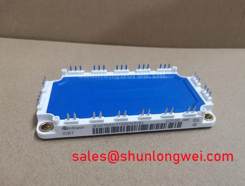
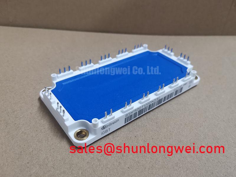
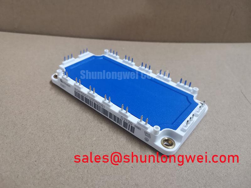
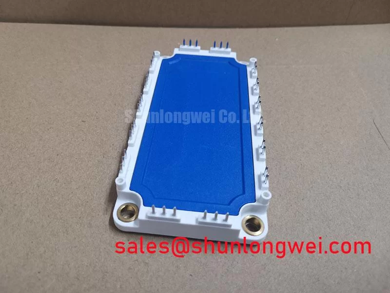
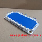
With the traction inverter isolated, measure the gate-to-emitter resistance at the disconnected driver harness before reconnecting it to the BSM150GT120DN2-6. Record the result against a known-good assembly, then confirm the driver’s output connections against the equipment schematic. The Infineon part is a 1200 V, 150 A IGBT module (Official Specification); those ratings do not identify its gate-drive voltage, pin assignment, or isolation requirements.
In an electric material-handling vehicle, the high-side driver supply must remain within the driver and module operating limits as its emitter potential moves with the switching node. As a Design Consideration, size the isolated DC-DC supply from the selected driver’s consumption, switching demand, and measured gate-charge behavior rather than from the module’s current rating. Check supply regulation during commanded switching and during undervoltage lockout. A supply that looks stable at idle may behave differently when the inverter is pulsing.
Isolation-barrier rating, creepage, clearance, and common-mode transient immunity belong to the selected driver, power supply, PCB, and complete installation. Do not assign a reinforced-isolation or CMTI rating to this IGBT module on the strength of its voltage rating. The system designer should verify those requirements against the vehicle’s electrical architecture and the relevant component documentation. If an unexpected gate pulse appears during switching, compare the driver input, isolated supply, and gate-to-emitter waveform with a known-good channel before changing components.
Keep the driver return close to its associated gate path as a Design Consideration, and confirm whether the module’s documented terminals provide a dedicated auxiliary emitter before routing one. An assumed Kelvin connection can invalidate a carefully laid-out driver board. Miller-current control, active clamping, and gate-loop damping are driver-level choices to validate with measured switching waveforms; none should be treated as a built-in feature of the BSM150GT120DN2-6 without supporting documentation.
Thermal Time Constants (tau_i) and Peak Junction Temperature Margin Calculation
Start a pulsed-load assessment with the actual forklift duty trace: capture DC-link voltage, module current, switching activity, case temperature, and cooling conditions through acceleration, lifting, and repeated low-speed operation. The 150 A rating (Official Specification) is an identification and selection boundary, not permission to carry that current under every case temperature or pulse pattern. Junction-temperature limits, transient thermal impedance, and loss curves must come from the applicable manufacturer documentation before a numerical margin can be claimed.
For a module with documented multi-RC thermal data, an Engineering Calculation applies the measured loss waveform to the thermal response and adds the resulting junction-to-case rise to the measured case temperature. Each thermal time constant contributes differently as pulses lengthen or repeat. A cold heatsink reading taken between events cannot, by itself, establish the peak junction temperature reached during an overload. If the necessary thermal curves are unavailable, retain the assessment as an unresolved design check rather than substituting another package’s values.
Short-circuit protection needs a separate review. Check the driver schematic for desaturation detection, blanking behavior, and controlled turn-off, then compare those functions with the module’s documented short-circuit limits and safe operating conditions. During a fault, a fast interruption can produce a substantial turn-off overshoot; a controlled turn-off is not evidence that the semiconductor remains within its voltage or thermal limits. Validate the complete protection sequence under a test plan appropriate to the equipment.
Parallel modules add a sharing question to the thermal calculation. Compare their measured on-state behavior under comparable temperature and drive conditions, and examine the documented temperature dependence of collector-emitter saturation voltage before relying on any self-balancing effect. Equal nominal current ratings do not prove equal current division. Busbar resistance, cooling differences, and gate-loop timing can shift losses from one position to another, particularly during short traction-current peaks.
Optimizing Heatsink Contact Pressure and Surface Roughness for Minimum R_th(c-s)
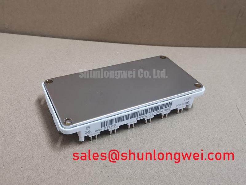
Before mounting the replacement module, inspect the heatsink seating area for burrs, embedded debris, corrosion, and old thermal compound. Check flatness and surface finish against the module and interface-material instructions. The aim is continuous thermal contact without using screw force to pull a distorted surface into place. Case-to-heatsink thermal resistance depends on the assembled joint; it is not established by the module’s 1200 V rating (Official Specification) or by how tightly the screws feel during installation.
Apply the thermal interface material using the approved process for that material and mounting arrangement. As a Design Consideration, control coverage and finished bond-line thickness so that exposed gaps and excessive compound are avoided. A universal grease thickness or mounting torque should not be imposed on the BSM150GT120DN2-6 without its mechanical specification. Seat the module evenly, tighten fasteners in the prescribed sequence, and use the specified hardware and torque where those instructions are available. Record the compound, heatsink condition, and fastening method so a later thermal comparison has a meaningful baseline.
💡 Pro Tip: Verify the module-specific mounting torque before tightening, because a generic fastener setting cannot confirm correct baseplate contact pressure.
If case temperature rises unusually during a repeatable duty test, compare airflow or coolant conditions, heatsink temperature, fastening condition, and the thermal interface before attributing the result to the semiconductor. A contact problem and an increased electrical loss can produce similar external temperature symptoms. Use simultaneous electrical and thermal measurements to separate them.
Symmetrical Busbar Geometry for High-Current Parallel Module Arrays
Trace the positive and negative DC-link paths through each module position before fitting a parallel array. Match their current-path geometry and connection resistance as a Design Consideration, then verify current sharing under the vehicle’s actual switching and load conditions. A laminated busbar can help reduce loop inductance, but its physical symmetry matters: unequal paths may expose one module to greater turn-off overshoot or current. Measure collector-emitter voltage at switching with a suitable high-voltage setup and compare the observed peak with the documented device limit.
Gate paths deserve the same positional comparison. Keep each gate conductor paired with its correct emitter return, inspect the driver schematic for individual damping and protection arrangements, and compare gate-to-emitter waveforms across positions. The Miller plateau and reverse-transfer effects can influence switching behavior, but no module-specific charge or capacitance value should be inferred from the part number. If one position oscillates or switches later, investigate its wiring and measurement reference before changing driver settings across the array.
For a repair evaluation, FF150R12ME3G is a separate module candidate to assess, not a confirmed drop-in replacement. Compare its terminal map, mechanical interface, gate-drive requirements, thermal data, and protection limits with both the BSM150GT120DN2-6 documentation and the original inverter design. Infineon’s EasyPACK module information illustrates why package families require their own mounting and connection checks; its specifications must not be transferred to this module. Likewise, Infineon’s low-voltage MOSFET range addresses a different device class and does not establish IGBT gate-drive limits.
When investigating unequal switching or a failed inverter position, preserve the original wiring layout, log measurements against a functioning channel, and work outward from the gate signal to the DC-link and cooling paths. The Field Engineer’s Handbook provides a broader testing and failure-analysis framework; the final compatibility decision still depends on the module documentation and measurements from the specific traction inverter.