

Content last revised on September 25, 2026
Fuji Electric 2MBI450VX-120-50 Overview
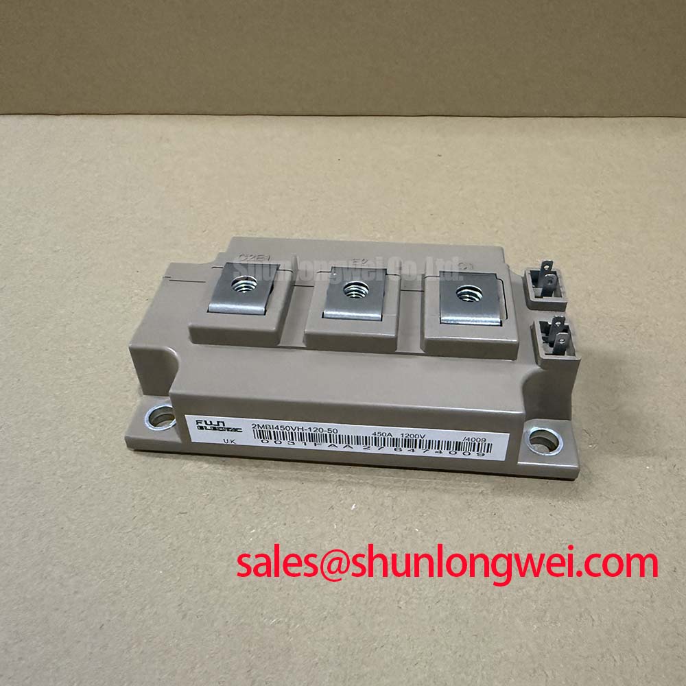
Before energizing a replacement, inspect the module body and terminals, then verify the nameplate boundary against the converter design: VCES = 1200 V and IC = 450 A at TC = 80°C are the key Fuji Electric ratings for the 2MBI450VX-120-50.
The 2MBI450VX-120-50 is a high-current Fuji Electric IGBT module intended for power conversion systems where switching behavior, thermal impedance, gate-loop control, and mechanical mounting must be validated together. Its official electrical data includes a collector power dissipation of 2305 W, a maximum specified junction temperature of +150°C, and a specified VCE(sat) of 1.85 V at IC = 450 A. These values describe the device boundary under stated test conditions; they do not replace system-level switching, thermal, or insulation validation.
| Parameter | Official Specification |
| Manufacturer | Fuji Electric |
| Model | 2MBI450VX-120-50 |
| Collector-emitter voltage | 1200 V |
| Continuous collector current | 450 A at TC = 80°C |
| Collector power dissipation | 2305 W under datasheet conditions |
| Operating junction temperature | Up to +150°C |
| VCE(sat) | 1.85 V at IC = 450 A |
| Gate-emitter threshold voltage | 6.5 V |
| Input capacitance | 37 nF |
| Thermal resistance | Rth(j-c) = 0.065 K/W for the IGBT |
Benchtop Waveform Tuning: Mitigating Stress via Common-Mode Transient Immunity on 2MBI450VX-120-50
Begin bench work with the power stage isolated and the gate-drive supply disabled. Confirm the driver reference, gate-emitter return, and auxiliary control connection against the original inverter schematic before applying a switching pulse. The module’s official VGE(th) rating is 6.5 V, but threshold voltage is not a recommended turn-on level and should not be treated as a noise margin. Gate voltage, pulse width, dead time, and turn-off behavior must be assessed with the actual driver and bus structure.
For a utility-scale 1500 V high-power central solar photovoltaic inverter, the first compatibility question is the DC-link topology. A 1200 V collector-emitter rating does not by itself establish suitability for a 1500 V bus. Designers should verify the actual semiconductor voltage stress, switching overshoot, transient suppression network, and operating derating against the converter’s maximum DC-link condition. A 1500 V photovoltaic inverter may require a different voltage class or a validated clamped topology; this decision belongs to the system engineer after double-pulse and fault-condition testing.
Common-mode transients can couple through the isolated driver barrier, gate wiring, heatsink structure, and measurement equipment. When the design specification calls for reinforced galvanic isolation above 5 kV or common-mode transient immunity above 100 kV/µs, those figures should be verified from the selected driver documentation and the complete isolated power-stage design. They are not official specifications of this Fuji Electric IGBT module. Use a differential probe with suitable common-mode capability, observe both gate-emitter voltage and collector-emitter behavior, and compare the waveform with the driver’s commanded state.
Dead-time protection should be confirmed at the actual operating temperature and load rather than only at room-temperature bench conditions. The practical objective is to prevent cross-conduction while avoiding excessive diode conduction and recovery stress. A short, controlled gate loop and a low-inductance driver return help reduce ringing, while a gate resistor and damping network should be selected through measured waveform tuning. A microsecond-scale gate buffer or interlock delay may be appropriate in some system architectures, but its value is determined by driver propagation delay, pulse-width requirements, and the measured switching transition.
If an unexpected gate pulse appears, separate the investigation into command-side timing, isolated power supply behavior, probe loading, and common-mode current paths. Check the gate-emitter waveform at the module terminals rather than at a remote driver test point. The external reference on Wide Bandgap Revolution also provides useful background for comparing switching-edge control and parasitic-inductance challenges across power semiconductor technologies.
Transient Dynamics & Electrical Design: Baseplate Convexity Compensation and Screw Control
The thermal path should be prepared before the module is bolted into the converter. Clean the heatsink contact area, inspect the baseplate and mounting surface for contamination, and apply the selected thermal interface material according to its manufacturer’s process window. A controlled, uniform layer is preferable to excessive compound, trapped air, or local dry areas. A 50 to 100 µm interface target may be used only where it is supported by the chosen TIM process and surface condition; it is a design consideration, not an official specification of the 2MBI450VX-120-50.
Baseplate curvature and heatsink flatness can influence contact pressure across the active thermal area. Designers should verify the mating surfaces and use the manufacturer’s approved mounting sequence, hardware, and torque data. Tighten progressively in a cross-pattern so that the baseplate is not pulled unevenly against the heatsink. If spring washers or disc springs are used to stabilize contact pressure, their compression, tolerances, and temperature behavior must be calibrated for the actual fastener stack rather than assumed from a generic torque value.
💡 Pro Tip: Do not treat mounting torque as a substitute for thermal verification; check the assembled interface through temperature measurement and confirm that the measured case temperature remains consistent with the calculated power loss.
The official Rth(j-c) value is 0.065 K/W for the IGBT, but the complete thermal path also includes interface resistance, heatsink resistance, airflow, clamping uniformity, and transient load profile. The specified Pc of 2305 W should therefore be read with its test conditions and temperature assumptions, not as a continuous field operating promise. Thermal calculations should use measured case temperature and the actual switching and conduction losses of the application.
When multiple modules operate in parallel, symmetrical busbar geometry and matched electrical path length are important design considerations. The positive temperature coefficient associated with VCE(sat) can support static current sharing at operating temperature, but it does not guarantee dynamic sharing during turn-on or turn-off. Verify current balance with appropriately rated current probes while checking collector-emitter overshoot and gate timing across every parallel path.
Transient Dynamics & Electrical Design: PCB Symmetry Considerations for Dual IGBT
In a dual-IGBT power assembly, the main high-current emitter path and the gate-drive return should be treated as separate functions. Route the control return to the designated auxiliary emitter or control reference defined by the applicable module documentation, while keeping it away from the high di/dt power emitter conductor. The purpose is to prevent voltage developed by common emitter impedance from appearing as a false gate signal.
Symmetry matters on both the PCB and the busbar. Keep corresponding gate paths similar in length and geometry, avoid routing one channel beside a noisy collector node, and place the gate resistor and any damping components close to the module connection. The power loop should be compact, but the control loop must not borrow the power return simply because it is physically convenient. Any auxiliary terminal assignment should be checked against the original Fuji Electric documentation before layout release.
During troubleshooting, measure the gate-emitter waveform directly at each module channel and compare turn-on delay, turn-off slope, ringing, and plateau behavior. If one channel differs, inspect connector contact resistance, driver supply decoupling, gate resistor placement, and return-current routing before changing the switching command. An apparent oscillation may involve probe reference inductance, driver instability, parasitic coupling, or unequal power-loop impedance, so the waveform should be compared with a known-good signal path under the same test conditions.
Gate dielectric stress also deserves controlled treatment. Negative bias, excessive ringing, and prolonged high-temperature operation can affect semiconductor gate structures. Do not infer service life, failure rate, or safe negative gate voltage without an applicable Fuji Electric specification or qualified test source.
For replacement assessment, compare the original circuit’s voltage class, current test condition, gate-drive requirements, thermal interface, terminal arrangement, and switching frequency. The 2MBI400U4H-170 may be reviewed as a separate engineering candidate, but its different rating set and mechanical or electrical interface must be validated independently rather than assumed interchangeable.
2MBI450VX-120-50 Thermal-Electrical Optimization: Thermal Feedback Practical Tuning
Thermal optimization starts with separating conduction loss from switching loss. The official VCE(sat) value of 1.85 V at 450 A is a reference point for conduction-loss evaluation under the stated test condition. Actual loss varies with collector current, junction temperature, gate-drive condition, switching speed, diode behavior, and commutation path. Use measured current and voltage waveforms to establish the application loss model instead of multiplying the headline rating by an assumed duty cycle.
The positive temperature behavior of VCE(sat) can help stabilize steady-state current sharing between paralleled devices, because a warmer path may develop greater conduction voltage and naturally discourage additional current. This effect is conditional and does not correct unequal gate timing, unequal busbar impedance, or different thermal contact. Match gate-loop wiring, power-path resistance, and cooling conditions, then confirm balance at low, nominal, and high operating temperatures.
The input capacitance specification of Cies = 37 nF is useful when reviewing driver loading, but capacitance alone does not determine switching time. Gate charge, driver output impedance, gate resistance, Miller coupling, and commutation voltage all influence the actual waveform. Designers should tune the gate network from measured collector-emitter and gate-emitter traces, maintaining sufficient dead time to prevent shoot-through while checking that excessive delay does not increase diode recovery or conduction stress.
Overvoltage control should combine minimized commutation-loop inductance with a properly selected clamp and absorption network. A MOV may be coordinated with other suppression components where the system energy, repetitive pulse duty, clamping voltage, and thermal behavior support that arrangement. The MOV rating and placement are system decisions; they must be verified against the converter’s maximum voltage, fault energy, and switching transient measurements rather than selected from the IGBT voltage rating alone.
For field diagnosis, record case temperature, coolant or airflow condition, gate waveform, collector-emitter overshoot, switching frequency, and load current at the same operating point. A temperature rise or waveform change may result from several interacting conditions, including interface pressure, driver timing, busbar asymmetry, sensor placement, or altered load impedance. Controlled comparison with the original assembly gives the repair engineer a more reliable basis for deciding whether the 2MBI450VX-120-50 is electrically and mechanically compatible with the target inverter.