


Content last revised on March 26, 2026
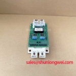
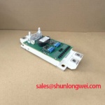
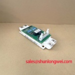
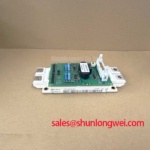
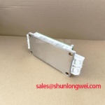
2SP0115T2A0-17 Power Integrations 1700V Dual-Channel SCALE-2 Gate Driver
The 2SP0115T2A0-17, a cornerstone of the Power Integrations SCALE-2 family, is a highly integrated, dual-channel plug-and-play gate driver specifically optimized for 1700V PrimePACK™ IGBT modules. By consolidating the gate drive stage, isolated DC/DC converter, and comprehensive protection circuitry into a single compact footprint, it addresses the fundamental challenges of thermal management and switching reliability in high-power industrial environments. This driver is not just an interface; it is a dedicated control solution that ensures the IGBT operates within its safe operating area even under extreme transient conditions.
For high-power inverter designs prioritizing thermal margin and switching precision, the 2SP0115T2A0-17 1700V gate driver is the optimal choice. It effectively resolves the "invisible problem" of voltage overshoots during high-current turn-off through integrated Active Clamping. This mechanism limits the collector-emitter voltage, allowing engineers to push system performance without risking catastrophic semiconductor failure. What is the primary benefit of its integrated DC/DC converter? It eliminates the need for external isolated power supplies, significantly increasing power density and reducing PCB complexity.
Key Parameter Overview
Decoding the Specs for Enhanced Thermal and Switching Reliability
The following technical specifications are derived from official documentation to assist in precise system integration. The 2SP0115T2A0-17 is designed to provide a stable ±15A peak output current, ensuring rapid charging and discharging of the gate capacitance for the largest 1700V modules.
| Core Parameter | Specification Value | Engineering Significance |
| Max. Blocking Voltage | 1700V | Supports 690V AC grid applications with ample safety margin. |
| Peak Output Current | ±15A | Enables high-speed switching for modules up to 1400A. |
| Number of Channels | 2 | Dual-channel design for half-bridge drive synchronization. |
| Integrated DC/DC Power | 1.2W per channel | Sufficient overhead for high-frequency switching operations. |
| Interface Logic | 15V Electrical | Standard industrial logic compatibility for noise immunity. |
| Protection Features | Vce Monitoring / Active Clamping | Dual-layer defense against short-circuits and overvoltage. |
Download the 2SP0115T2A0-17 datasheet for detailed specifications and performance curves.
Application Scenarios & Value
Achieving System-Level Benefits in High-Power Conversion
In high-fidelity engineering scenarios, such as Wind Power Inverters or Centralized Solar Inverters, the 2SP0115T2A0-17 plays a decisive role in maintaining Power Cycling Capability. Consider a wind turbine system facing rapid wind speed fluctuations; the resulting load changes create thermal stress on the IGBT. This driver manages those transitions by providing consistent gate signals, minimizing switching losses and preventing localized hot spots on the silicon die.
The 2SP0115T2A0-17 is frequently utilized in Variable Frequency Drives (VFD) and heavy-duty Servo Drive systems where Short-Circuit Withstand Time is critical. Its Vce Monitoring detects desaturation in microseconds, initiating a controlled turn-off before the energy levels exceed the module's SCSOA (Short Circuit Safe Operating Area). This level of protection is essential for maintaining a low Total Cost of Ownership (TCO) in industrial automation. For systems requiring even higher power handling or different topologies, the 2SP0320TC0-17 offers extended current capabilities while maintaining the same 1700V reliability standards. For the power stage itself, engineers often pair this driver with high-performance modules like the FF600R17ME4 to achieve an optimized balance of efficiency and durability.
Technical & Design Deep Dive
A Closer Look at the SCALE-2 Architecture for Long-Term Reliability
The technical superiority of the 2SP0115T2A0-17 stems from its SCALE-2 chipset, which reduces the component count by up to 80% compared to discrete solutions. This massive reduction in parts directly correlates to an increase in MTBF (Mean Time Between Failures). Think of the SCALE-2 chipset as the "brain" of the driver; it manages the timing between the two channels with sub-nanosecond precision, preventing shoot-through currents in the half-bridge. This is analogous to a precision-timed engine valve system; if the timing is off by a fraction, the entire system risks destruction.
Furthermore, the Active Clamping feature acts as a high-speed "pressure relief valve" for voltage. During a turn-off event, the stray inductance in the DC link can cause a voltage spike. The 2SP0115T2A0-17 monitors this and partially re-opens the IGBT if the voltage exceeds a set threshold, safely dissipating the energy. This allows designers to use a smaller Snubber Circuit, saving space and cost while improving Switching Efficiency. For a deeper understanding of these principles, engineers can refer to our guide on robust gate drive design or explore the in-depth analysis of IGBT modules.
Frequently Asked Questions
How does the Vce desaturation monitoring in the 2SP0115T2A0-17 protect against short circuits?
The driver continuously monitors the Vce(sat) voltage across the IGBT during the "on" state. If a short circuit occurs, the Vce rises rapidly. Once it crosses the pre-defined threshold, the 2SP0115T2A0-17 immediately shuts down the gate signal to prevent the IGBT from entering a destructive thermal runaway state.
What is the impact of the ±15A peak current on large PrimePACK™ modules?
Large modules have high gate charge (Qg). A peak current of ±15A ensures that the gate voltage reaches its target quickly, reducing the time the IGBT spends in the linear region. This directly lowers Switching Loss and prevents the driver from overheating during high-frequency operation.
Does the 2SP0115T2A0-17 require a negative gate voltage supply?
No. The 2SP0115T2A0-17 features an integrated DC/DC converter that generates the necessary positive and Negative Gate Voltage internally. This ensures a robust turn-off and provides high immunity against parasitic turn-on caused by the Miller Clamp effect in high-power applications.
As the global energy landscape shifts toward electrification, the demand for reliable power conversion is paramount. Solutions like the 2SP0115T2A0-17 provide the technical foundation for the next generation of Electric Vehicle (EV) Inverters and grid-scale storage, ensuring that high-power semiconductors deliver their maximum potential with uncompromising safety.