Content last revised on January 25, 2026
2SP0320TC0-17: Advanced IGBT Gate Driver for 1700V High-Efficiency Power Conversion
Precision Control for Demanding High-Voltage Applications
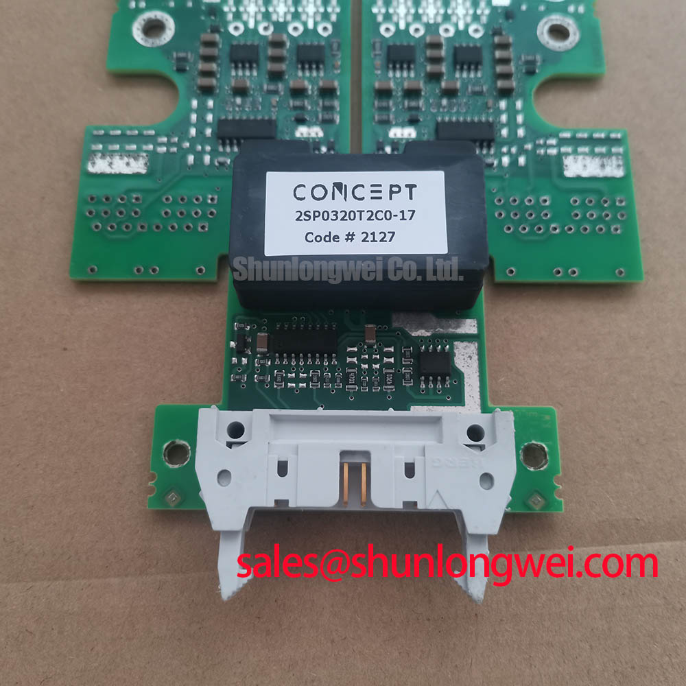
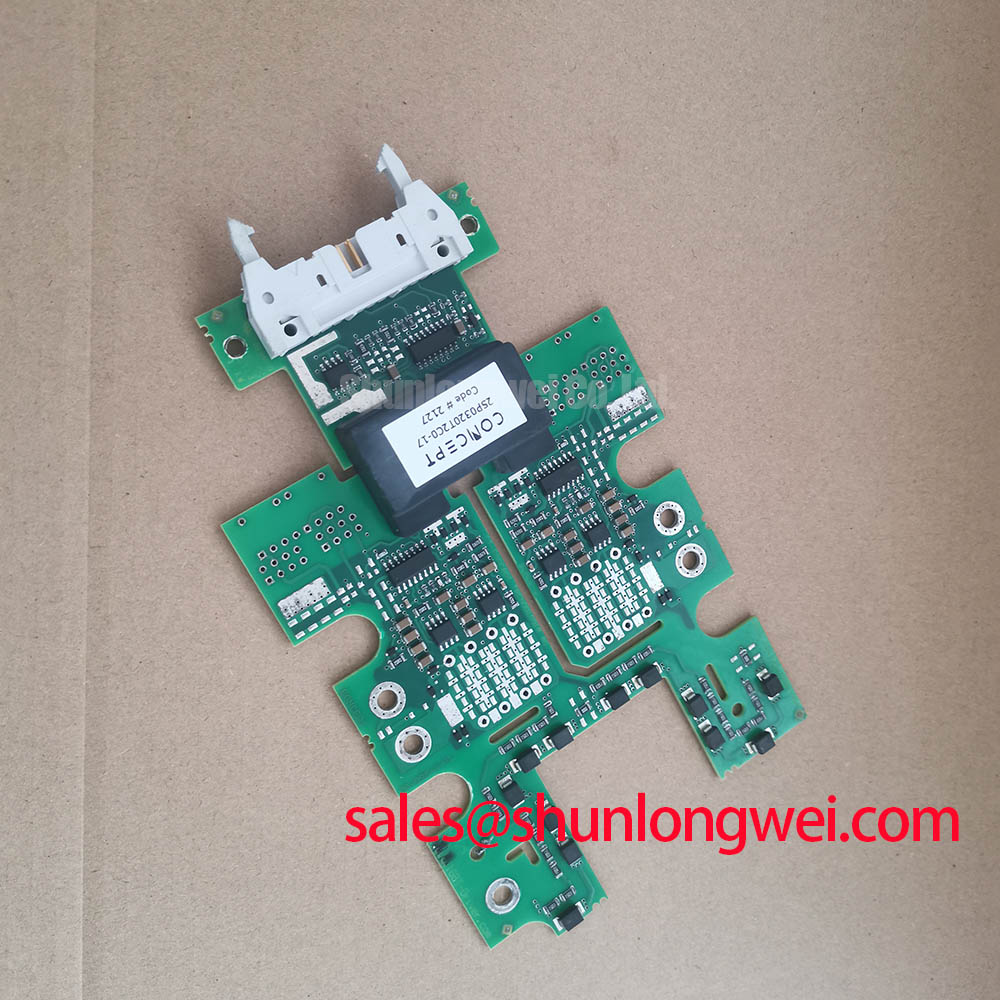
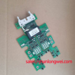
The 2SP0320TC0-17 from Power Integrations is a dual-channel SCALE-2 plug-and-play gate driver engineered to maximize the performance and reliability of 1700V IGBT modules. This driver delivers precise switching control through advanced features, enabling significant reductions in switching losses and enhancing overall system safety. Key specifications include: 1700V Blocking Voltage | ±20A Peak Output Current | Integrated Active Clamping. The core engineering benefits are superior IGBT protection and simplified system design. It directly addresses the challenge of safely driving high-voltage IGBTs at high frequencies by providing a fully integrated solution with VCEsat monitoring and a fast, reliable short-circuit response. For engineers developing high-power inverters, the 2SP0320TC0-17's integrated protection mechanisms make it the optimal choice for improving system robustness without complex external circuitry.
Key Parameter Overview
Decoding the Specs for Enhanced Switching Performance
The technical specifications of the 2SP0320TC0-17 are tailored to deliver robust and efficient control of high-power IGBT modules. The following table highlights key parameters and interprets their direct impact on system design and reliability.
| Parameter | Typical Value | Engineering Value & Interpretation |
|---|---|---|
| Max. Blocking Voltage | 1700V | System Voltage Compatibility: Directly matches the voltage class of 1700V IGBTs, making it suitable for applications in 1000V to 1200V DC-link voltage systems, common in renewable energy and industrial drives. |
| Peak Gate Output Current (Iout,peak) | ±20A | Switching Speed & Efficiency: A high peak current ensures rapid charging and discharging of the IGBT's gate capacitance. This is analogous to having a powerful engine in a car for quick acceleration; it enables faster turn-on and turn-off, which directly reduces Switching Loss and improves thermal performance. |
| Turn-on/Turn-off Delay Time (td(on)/td(off)) | ~100 ns | Control Precision: Extremely low and well-matched delay times across channels are critical for minimizing dead-time in half-bridge configurations, reducing distortion and improving the efficiency of inverter output waveforms. |
| Short-Circuit Protection Response Time | < 10 µs | Device Safety: Provides a rapid response to desaturation events, turning off the IGBT well within its SCSOA (Short Circuit Safe Operating Area) to prevent catastrophic failure. This is a critical safety feature for system reliability. |
| Isolation Voltage (Viso) | 4000VAC (1 min, 50Hz) | Operator Safety & Noise Immunity: High galvanic isolation safely separates the low-voltage control logic from the high-power output stage, ensuring user safety and preventing high-voltage noise from disrupting sensitive control circuits. |
Application Scenarios & Value
Achieving System-Level Benefits in High-Power Converters
The 2SP0320TC0-17 is specifically designed for high-reliability applications where efficient control of 1700V IGBTs is paramount. Its plug-and-play nature significantly accelerates the development cycle for engineers working on complex power systems. What is the primary benefit of its integrated protection? It drastically simplifies the gate drive design, eliminating the need for separate desaturation detection and active clamping circuits.
A high-fidelity engineering scenario is its use in a wind turbine power converter. These systems experience fluctuating loads and are exposed to harsh environmental conditions. The 2SP0320TC0-17's integrated Active Clamping feature is critical here. During IGBT turn-off, it actively limits the Vce voltage spike caused by stray inductances, preventing the IGBT from exceeding its breakdown voltage. This robust protection ensures the converter operates reliably even under transient overvoltage conditions, maximizing energy uptime and converter lifespan. This driver is also well-suited for industrial Variable Frequency Drive (VFD) systems and large-scale Solar Inverter applications where uptime and device protection are non-negotiable. For systems requiring a different feature set or interface, the related 2ED300C17-ST provides an alternative driver solution.
Technical Deep Dive
A Closer Look at Active Clamping for Enhanced Reliability
The Active Clamping function integrated into the 2SP0320TC0-17 is a cornerstone of its protective capabilities. In high-power switching, parasitic inductance in the busbar structure is unavoidable. When an IGBT turns off, this inductance causes a significant voltage overshoot across the collector-emitter terminals (Vce). If unmanaged, this spike can easily exceed the IGBT's maximum voltage rating, leading to immediate failure. The Active Clamping circuit acts like a sophisticated pressure relief valve. It constantly monitors the Vce voltage. If the voltage attempts to exceed a predefined threshold during turn-off, the clamping circuit provides a feedback path to the gate, momentarily slowing the turn-off process just enough to safely dissipate the inductive energy without allowing the voltage to reach a destructive level. This feature is particularly valuable as it allows designers to push for faster switching speeds to reduce losses, secure in the knowledge that a robust, active protection mechanism is in place to handle the resulting voltage transients.
Frequently Asked Questions (FAQ)
What is the main advantage of the SCALE-2 chipset used in the 2SP0320TC0-17?
The highly integrated SCALE-2 chipset reduces the external component count by up to 80% compared to conventional gate driver designs. This simplification significantly increases mean time between failures (MTBF) and enhances overall system reliability.
How does the VCEsat monitoring feature protect the IGBT module?
The driver continuously monitors the IGBT's collector-emitter saturation voltage (VCEsat) during the on-state. An abnormally high VCEsat indicates a short-circuit or overload condition. Upon detection, the driver initiates a safe and controlled shutdown of the IGBT in under 10 microseconds, preventing catastrophic failure.
Are the gate resistors for the 2SP0320TC0-17 fixed?
No, the turn-on (Rg,on) and turn-off (Rg,off) gate resistors are intentionally not assembled on the board. This provides maximum flexibility for the design engineer to select optimal resistor values to fine-tune switching speed, control EMI, and manage voltage overshoots (dv/dt) for their specific IGBT module and application layout.
Can this driver be used for paralleling IGBT modules?
Yes, the SCALE-2 architecture is designed to support direct paralleling of multiple IGBT modules. The high precision of the drivers ensures minimal delay time variance between channels and drivers, which is crucial for balanced current sharing among the paralleled modules.
What does the "T" in the part number 2SP0320TC0-17 signify?
The "T" typically refers to the electrical interface type of the driver. This model uses a standard 20-pin flat cable electrical interface for power and control signals, which is common in many industrial applications for its simplicity and reliability.
Engineering Perspective on System Integration
From an engineer's viewpoint, the 2SP0320TC0-17 is more than a component; it is a system-level solution. By integrating a DC/DC power supply, advanced protection features, and a high-isolation barrier into a single plug-and-play unit, it abstracts away much of the complexity and risk associated with high-voltage Gate Drive design. This allows design teams to focus their resources on core application logic and system optimization, rather than on the intricacies of gate drive circuitry. The result is a faster time-to-market, a more reliable end product, and a simplified supply chain.


