




Content last revised on October 13, 2026
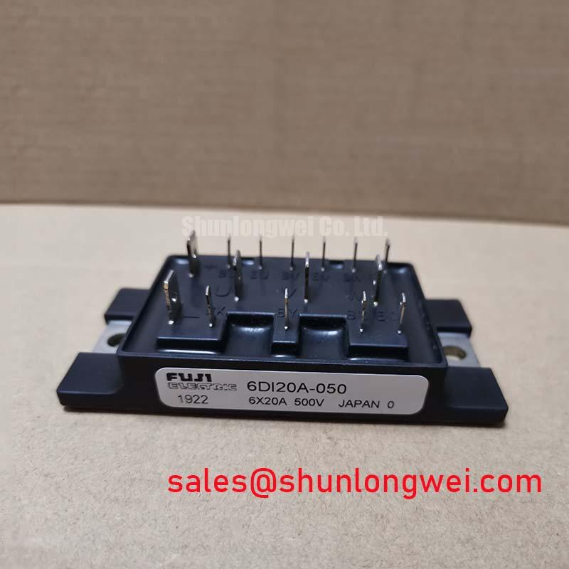
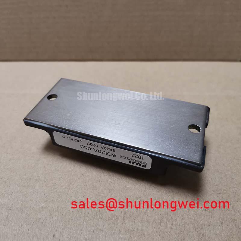
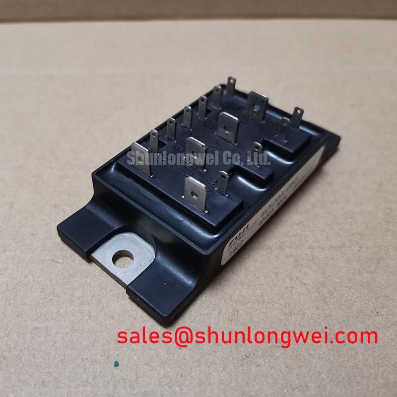
Transient Dynamics & Electrical Design: Preventing Spurious Power-Up Shoot-Through on 6DI20A-050
Check that the driver remains inhibited while its auxiliary supply rises, falls, or recovers from an interruption. As a Design Consideration, DC-link enable should depend on established driver readiness rather than simply the presence of a control command. Observe the driver supply, inhibit signal, and transistor control waveform together, using probes appropriate to the circuit potential.
The relevant distinction is base current and stored charge. Negative IGBT gate-bias prescriptions, gate-charge calculations, and Miller-clamp settings cannot be transferred directly to this Darlington module. Designers should evaluate the existing base-drive network, its turn-off extraction path, and the interval between opposing transistor commands against the device characteristics and equipment schematic. A driver undervoltage condition should leave the power stage inhibited rather than partially driven.
If unwanted conduction appears during startup, compare the command signals with the actual base-emitter waveforms. Supply ramp behavior, floating control connections, and coupled switching noise are separate possibilities; none should be diagnosed from a single waveform alone. Maintain separation between sensitive control conductors and switched power nodes, with electrical clearance determined by the assembly’s working voltage and applicable equipment requirements.
Fuji Electric’s High-Speed Discrete IGBTs documentation provides context for a different device family, not operating limits for the 6DI20A-050. That distinction matters when an existing driver board is being evaluated alongside newer semiconductor technologies.
6DI20A-050 Circuit Protection & Reliability: Evaluating Type-2 Coordination for the Power Transistor Module
Evaluate the semiconductor fuse against the actual prospective fault current, DC interruption capability, and protection arrangement before accepting its coordination with the module. As a Design Consideration, total clearing I²t alone does not establish transistor survival or prevention of enclosure rupture. The assessment also needs device withstand information, fuse clearing behavior, and equipment-level fault testing; Type-2 coordination is not a standalone module rating.
Review the high-side driver supply throughout its longest commanded conduction interval. If the equipment uses a bootstrap supply, assess capacitance from the drive circuit’s current demand, auxiliary consumption, leakage, permissible supply droop, and available recharge time. For this Darlington stage, an IGBT gate-charge-only calculation would overlook sustained base-drive demand.
Replacement assessment should start with terminal mapping, drive requirements, mounting geometry, and thermal performance. The 6DI50AH-050 is a comparison candidate, not an established direct replacement solely because its designation resembles the 6DI20A-050.
| Selection checkpoint | 6DI20A-050 | 6DI50AH-050 |
|---|---|---|
| Manufacturer | Fuji Electric | Consult datasheet |
| Rated current | 20.0 A — consult datasheet for rating conditions | Consult datasheet |
| Package classification | Power Transistor Module | Consult datasheet |
| Voltage rating and terminal geometry | Consult datasheet | Consult datasheet |
| Replacement status | Reference device | Requires electrical and mechanical comparison |
When evaluating compatibility with a compact industrial inverter or high-speed CNC spindle drive, inspect each power-stage function separately. The 6MBI75S-120-01 belongs in a separate IGBT-stage assessment, not an assumed front-end rectifier position. Fuji Electric’s PIM 7-Pack overview helps distinguish integrated power-stage arrangements from the discrete circuit functions surrounding this module.
Transient Dynamics & Electrical Design: PCB Base-Drive Loop Layout Symmetry on 6DI20A-050
Route the base-drive return so that high-current emitter-path voltage drops do not unnecessarily disturb the control reference. This is a Design Consideration for the external circuit; it does not establish that the module contains a separate Kelvin-emitter terminal. Follow the actual terminal drawing rather than importing an IGBT footprint convention.
Compare corresponding drive loops for routing length, return placement, and proximity to switched conductors. Investigate ringing with short probe connections and a suitable differential measurement arrangement before changing damping components. Select damping through circuit testing that checks both oscillation and switching loss, rather than imposing an arbitrary resistance.
Maintenance Note: Monitor terminal temperature trends and inspect cooling airflow during scheduled service, correcting loose connections only with the equipment isolated and according to its assembly instructions.
Include heatsink contamination, thermal-interface deterioration, and condensation evidence in the same inspection record. Set inspection intervals from cabinet conditions and temperature trends rather than assigning an unsupported module lifetime. The Industrial Applications reference offers broader integration context; use equipment-specific acceptance criteria for thermal and switching tests, not assumed altitude, cosmic-ray, or insulation guarantees.