


Content last revised on September 10, 2026
6DI85A-060 Thermal Electrical Optimization: DC Link Capacitance Bank Layout and Low Inductance Tuning
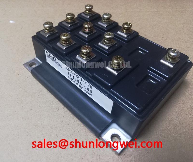
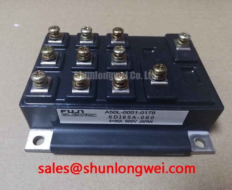
Before fitting the module, isolate the equipment, inspect the terminal area for heat discoloration or mechanical damage, and verify that the converter’s required voltage and current do not exceed the 600 V voltage rating and 85 A rated current of the Fuji Electric 6DI85A-060 under the applicable datasheet conditions. These are Official Datasheet Specifications for a Power Transistor Module; the original circuit documentation remains necessary to confirm terminal assignment, driver compatibility, and the intended converter topology.
| Parameter | Specification Status |
|---|---|
| Manufacturer | Fuji Electric |
| Part number | 6DI85A-060 |
| Rated voltage | 600 V Official Datasheet Specification |
| Rated current | 85 A Official Datasheet Specification under applicable conditions |
| Package category | Power Transistor Module |
DC link capacitor placement has a direct effect on switching overshoot because the peak device voltage rises with both parasitic loop inductance and current transition rate. As a Design Consideration, position the local capacitor bank so that the outgoing and return current paths remain closely coupled. A compact, symmetrical laminated or planar busbar arrangement can reduce loop area and help suppress turn off overshoot, while final voltage margins must be verified with switching waveform measurements at the actual operating current.
In industrial inverter welders and medium frequency induction heating power supplies, capacitor lead condition, busbar flatness, and terminal contact pressure should be checked together. A loose DC link connection can produce waveform ringing that resembles a gate drive issue. Where an auxiliary power stage is present, the 7MBR10KA060 is a related power module that engineers may review against its own published ratings and circuit requirements.
6DI85A-060 Operational Boundaries: Evaluating Regenerative DC Bus Voltage Surge Dissipation
When servicing a converter with a motor load or a rapidly changing induction heating load, capture the DC bus voltage during deceleration, load release, and fault shutdown. Regenerative energy can raise the bus voltage, and the 6DI85A-060 must remain within its 600 V specified voltage rating under measured operating conditions. The braking path, resistor assembly, control logic, and any external switching device are system level elements that require separate validation.
A braking transistor and ballast resistor should be assessed from the stored or returned energy, repetition pattern, cooling path, and protection response of the complete equipment. This is an Engineering Recommendation, not a published feature claim for this module. Inspect resistor terminations and thermal clearances, then compare captured bus waveforms with a known healthy unit where available. A persistent bus rise may involve the braking command, DC link capacitance, load dynamics, or measurement setup rather than one isolated component.
For module mounting, use an even, thin thermal interface material layer only after confirming the heatsink surface condition and the equipment manufacturer’s fastening requirements. 💡 Pro Tip: Tighten mounting hardware in a cross pattern so clamping force is distributed evenly, then verify thermal performance under the actual duty cycle rather than relying on installation appearance alone.
Benchtop Waveform Tuning: Mitigating Stress via Junction to Case Thermal Network Simulation on 6DI85A-060
Use a controlled bench test to compare gate command timing, collector or main switching node waveforms, DC bus ripple, and heatsink temperature before returning an inverter welder or induction heating supply to service. The 85 A rating is an Official Datasheet Specification, but allowable pulsed stress depends on the full operating condition, including switching losses, conduction losses, cooling effectiveness, and protection response.
Junction to case thermal modelling is a Design Consideration that helps engineers translate a pulsed loss profile into an estimated temperature excursion through the applicable transient thermal impedance data. The model must use manufacturer published thermal information for the exact module revision where available. It should not be replaced by an assumed continuous current calculation, particularly where welding output or heating power is cyclic.
Oscilloscope traces should be taken with probing methods suitable for fast switching nodes. Excessive ringing may indicate an interaction among busbar inductance, gate loop routing, snubber condition, and load cabling. Long motor or output cables can also create reflected voltage stress at the connected load; cable filtering and termination choices should therefore be evaluated at equipment level. Fuji Electric’s power semiconductor and IPM module information provides useful manufacturer context when reviewing applicable module families.
Where a different module family is being considered for repair evaluation, 6MBP100TEA060-50 should be compared objectively by voltage rating, current rating, package outline, terminal arrangement, gate drive requirements, cooling interface, and protection coordination. Physical interchangeability or electrical equivalence should not be assumed from nominal ratings alone.
6DI85A-060 Circuit Protection and Reliability: Calibrating Auxiliary Emitter Return Trace Separation
Inspect the gate drive return path before changing gate components. Shared impedance between a high current power return and the driver reference can alter the effective gate voltage during switching, potentially causing unstable transitions or false protection behaviour. As a Design Consideration, keep the driver return sensing path separate from the main high current emitter return wherever the original module pinout and driver architecture support that arrangement.
Gate loop inductance should be minimized to reduce susceptibility to Miller induced turn on and turn off oscillation. The final gate resistance, clamp approach, driver supply arrangement, and desaturation threshold are system determined values. Engineers should validate them with double pulse or equivalent controlled switching tests, checking peak voltage and current behaviour against the measured DC bus condition.
During fault investigation, inspect the driver board, isolation barriers, snubber components, DC link connections, output cable routing, and heatsink interface before attributing damage to the module alone. For broader context on how wide bandgap switching technologies introduce different layout and protection considerations, see Wide Bandgap Revolution.