

Content last revised on November 20, 2026
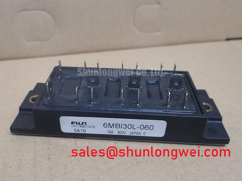
6MBI30L-060 Incoming Inspection and Product Identification
- Isolate the equipment, verify that the DC link is discharged, and identify the collector, emitter, and gate connections from the module terminal diagram before connecting test leads.
- Record cold-state diode-mode readings in both polarities across corresponding power paths, using consistent gate handling and the same meter settings.
- Check mounting-surface condition, terminal alignment, and fastener engagement before reconnecting conductors or applying mechanical load.
- Review the equipment’s insulation-test procedure and disconnect sensitive drive electronics before performing any permitted dielectric test.
The 6MBI30L-060 is a Fuji Electric IGBT module with specified ratings of 600.0 V collector-emitter voltage and 30.0 A continuous collector current. Its six-pack inverter arrangement makes terminal identification particularly important: comparable measurements must follow equivalent circuit paths, rather than simply adjacent physical terminals. For incoming inspection, preserve the connection map alongside the readings so subsequent comparisons remain meaningful.
When evaluating this module for light industrial automation or multi-joint robotic articulator drives, engineers should compare the existing inverter circuit, driver interface, mechanical footprint, and cooling arrangement. The model designation and headline ratings identify the component, but replacement acceptance also depends on the equipment’s electrical and mechanical interfaces.
| Parameter | Specified product information |
|---|---|
| Manufacturer | Fuji Electric |
| Part Number | 6MBI30L-060 |
| Product Category | IGBT Module |
| Collector-Emitter Voltage (Vces) | 600.0 V |
| Continuous Collector Current (Ic) | 30.0 A |
| Package | Fuji Power Module |
| Configuration / Topology | IGBT Power Stage |
| Circuit arrangement | 6-in-1 Six-Pack Inverter |
| Series | Standard |
| Additional acceptance limits | Consult Datasheet: terminal assignments, rating conditions, gate limits, insulation test conditions, thermal characteristics, dimensions, and fastening requirements. |
The voltage and current entries are component ratings, not an equipment operating prescription. In particular, the current rating must be interpreted with its specified thermal conditions. A diode-mode meter reading is a separate low-current observation; it should not be recorded as the module’s rated diode forward voltage or on-state collector-emitter voltage.
6MBI30L-060 Thermal-Electrical Optimization: Preventing Terminal Stress
Check conductor alignment before tightening the power connections so the terminal does not become the lever that pulls a misplaced busbar into position. As a Design Consideration, the conductor should meet its connection surface without forced bending, while surrounding supports absorb cable weight and assembly reaction. This reduces externally imposed stress without assuming any particular internal joint construction.
For threaded connections, compare the fastener length with the actual stack of conductor, washer, and terminal hardware. Engagement must satisfy the applicable assembly drawing without bottoming out or allowing hardware to contact unintended surfaces. A fastener that reaches its travel limit can produce an apparently firm connection without establishing the intended clamping condition. Check washer seating and contact-face cleanliness before treating a torque reading as evidence of a satisfactory joint.
Use the specified fastening method for the particular connection rather than transferring a torque value from another Fuji package. Terminal fasteners and baseplate mounting fasteners serve different mechanical functions. During assembly, support the mating conductor and prevent the module housing from taking the reaction load. After fitting surrounding covers or brackets, inspect for displaced conductors, reduced clearance, or contact with gate wiring.
Cooling-surface preparation deserves the same attention. As an Engineering Recommendation, inspect the heatsink mating area for raised burrs, contamination, and distortion before applying the approved thermal interface material. Its application method and bond-line control should follow the module and equipment assembly requirements. Excess material does not correct a distorted mounting surface, and tightening should not be used to pull a visibly misaligned assembly flat.
Cold electrical inspection is most useful when the fixture and handling method are repeatable. With the module isolated, use its circuit diagram to identify each accessible antiparallel diode path. Record forward and reverse observations with the same instrument, lead orientation, and temperature conditions. Differences between equivalent paths warrant further investigation; they do not, by themselves, establish a unique failure mechanism. Connected snubbers, driver boards, and parallel power paths can otherwise obscure the result.
💡 Bench Tip: Use ESD-controlled handling and consistent gate-to-emitter charge control when comparing cold diode-mode readings with a known-good reference.
For replacement evaluation, the 6MBI30F-060 is a comparison candidate, not an established drop-in substitute. Compare terminal mapping, mounting geometry, gate-drive requirements, switching characteristics, and thermal limits before approving either part against the equipment service specification. Retaining the original connection photographs and inspection record helps prevent a mechanically plausible substitution from bypassing an electrical compatibility check.
Preventing Spurious Faults: Mitigating Commutation Voltage Spikes in the 6MBI30L-060
Measure the collector-emitter switching waveform with a suitably rated differential measurement arrangement and a short, controlled probing loop. As a Design Consideration, distinguish actual overshoot from probe pickup before changing the driver or suppression network. Compare the waveform at relevant operating conditions, including DC-link level, load current, and device temperature, rather than relying on an unloaded switching trace.
Commutation involves both the switching transistor and the opposing freewheeling diode. Diode reverse recovery can increase the current handled by the turning-on transistor, while abrupt recovery can excite the power-loop parasitics. Peak reverse recovery current and recovery slope are operating-condition-dependent measurements, not values that can be inferred from the module’s current rating. Evaluate their contribution using properly synchronized current and voltage traces.
A turn-on gate-resistance adjustment can change the commutation rate, but it also changes switching loss. An RC snubber can damp a measured oscillation, but its resistor dissipation and capacitor stress must be evaluated within the actual circuit. As an Engineering Recommendation, base either intervention on the observed ringing, component loading, and thermal result; select final values through the system’s validation process rather than adopting a generic module recipe.
Keep outgoing and returning commutation paths closely coupled where the assembly permits, and avoid unnecessary separation between the local DC-link connection and the power stage. A laminated busbar arrangement can support this objective, but geometry alone does not establish the resulting inductance. Verify the assembled circuit’s peak voltage against the 600.0 V collector-emitter rating under the equipment’s relevant switching conditions.
Gate-loop observations should use the emitter reference associated with the gate connection, not an arbitrary chassis point. Common-mode displacement current and shared return impedance can alter the apparent gate voltage. As a Design Consideration, review gate-loop routing, driver return paths, and isolation capacitance when investigating unintended turn-on. If negative off-state bias is part of the existing driver, assess its waveform against the module’s gate limits; increasing its magnitude is not a universal noise remedy.
Switching-frequency changes also require a cooling review. Higher switching activity can raise switching losses even when output current remains similar. Compare stabilized case temperature, inlet-air condition, heatsink cleanliness, and airflow distribution across the assembly. Do not interpret a cool enclosure wall as evidence that the module’s thermal path is adequate, particularly where filters, neighboring heat sources, or fan condition affect local cooling.
Long motor leads introduce a separate measurement location: the motor terminals. Cable reflections can produce terminal peaks that differ from those measured at the inverter. As an Engineering Recommendation, assess cable characteristics and motor insulation requirements before choosing an output reactor or filter. Keep that assessment separate from the local snubber decision, which addresses the power stage’s commutation behavior rather than the complete cable transmission path.
6MBI30L-060 Circuit Protection & Reliability: Calibrating Junction-to-Case Thermal Network Simulations
Build the junction-to-case thermal model from applicable transient thermal-impedance information before evaluating a pulsed overload. As a Design Consideration, a multi-RC network should reproduce the relevant heating and cooling response across the pulse durations being investigated. Matching only steady-state thermal resistance does not establish that the model represents short-duration junction-temperature excursions.
For an Engineering Calculation, obtain instantaneous dissipation from the relevant electrical operating points and apply its time history to the thermal network. Combine the resulting junction-to-case temperature rise with the case-temperature boundary condition. Keep transistor and diode losses distinct where their loading differs, and represent repeated pulses rather than treating every overload as an isolated event from a fully cooled starting condition.
Calibration requires disciplined temperature measurement. Record the case measurement location, sensor attachment, heatsink condition, and operating sequence. Thermal interface resistance belongs in the case-to-heatsink path; it should not be silently absorbed into a junction-to-case model. Where the simulated and measured responses diverge, investigate sensor lag, boundary conditions, and loss assumptions before changing the thermal coefficients.
Protection timing needs a separate electrical assessment. Desaturation monitoring observes a collector-emitter voltage condition during commanded conduction; it is not a direct junction-temperature measurement. As an Engineering Recommendation, coordinate its detection behavior, blanking interval, and fault response with the actual driver and documented device limits. During soft shutdown, check that the changing current does not create an unacceptable collector-emitter transient.
Short-circuit acceptance must follow an applicable short-circuit operating-area specification and controlled test procedure. Neither a satisfactory cold diode check nor normal operation at rated current establishes short-circuit endurance. Preserve fault records and driver waveforms when investigating a trip, since supply disturbance, sensing behavior, and power-stage stress can require different corrective actions.
For broader context, AI, Energy, and IGBT discusses power-conversion considerations beyond this individual product. Fuji Electric’s 7th-Gen X-Series IGBT Modules and IGBT product resources provide manufacturer context for other device generations; their characteristics should not be transferred to the 6MBI30L-060.
Close the incoming-inspection record with the insulation procedure actually used, including the specified terminal grouping, test conditions, and acceptance criterion. Isolate connected electronics as required by the equipment procedure, and avoid substituting an improvised high-voltage test. For thermal release, retain the measured case-temperature trace, the modeled junction-temperature excursion, and the protection response together so acceptance rests on the assembled power stage’s behavior.