



Content last revised on September 29, 2026
1. Understanding Power Semiconductor Modules in Modern Energy Conversion
Modern electrical engineering relies heavily on power electronic conversion systems to bridge the gap between primary energy sources and demanding industrial loads. In adjustable speed motor drives, solar photovoltaic central inverters, uninterruptible power supplies (UPS), and industrial induction equipment, raw electrical power must be modulated with high precision and minimal energy loss. At the center of these power conversion systems is the Insulated-Gate Bipolar Transistor (IGBT), a solid-state switching device designed to overcome the physical limitations of earlier power semiconductors.
Historically, power engineers were forced to choose between the high current-carrying capacity of Bipolar Junction Transistors (BJTs) and the rapid, voltage-controlled switching speed of power Metal-Oxide-Semiconductor Field-Effect Transistors (MOSFETs). While power BJTs exhibit low on-state voltage drops during high-current conduction, they require substantial, continuous base currents to remain in saturation. This continuous base drive requirement introduces significant driving losses and necessitates complex drive circuitry. Conversely, power MOSFETs require virtually no continuous gate current due to their insulated capacitive gate structure, but their on-resistance increases dramatically as their breakdown voltage rating rises beyond 200V. The IGBT effectively merges these two structural concepts: it incorporates a voltage-driven MOS input gate to control a high-current bipolar conduction channel, thereby providing high input impedance, low driving power requirements, and superior current density at blocking voltages reaching hundreds or thousands of volts. Readers seeking a foundational overview of this architecture can explore Insulated-Gate Bipolar Transistor (IGBT) Fundamentals.
Within this technological domain, manufacturers package these semiconductor dies into modular power assemblies rather than discrete components. IGBT power modules mechanically consolidate multiple matched silicon dies—both active IGBT switches and antiparallel Free-Wheeling Diodes (FWDs)—onto an electrically isolated, thermally conductive substrate. This substrate, typically Direct Bonded Copper (DBC) ceramic bonded to a solid copper baseplate, serves two vital functions: it provides several kilovolts of galvanic isolation between the live electrical circuit and the grounded chassis heatsink, and it establishes a low-thermal-resistance path to carry heat away from the silicon junctions.
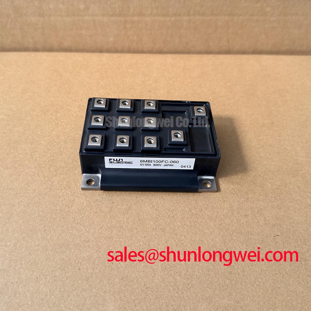
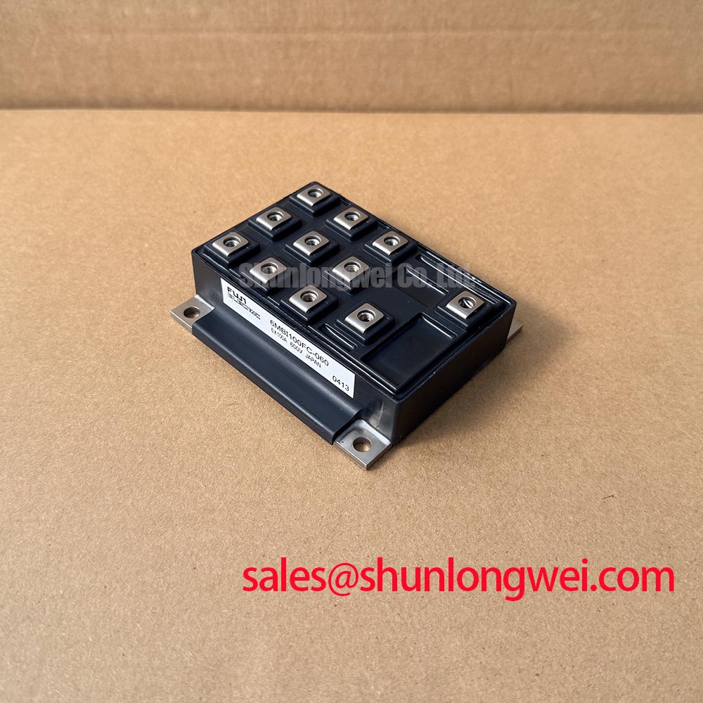
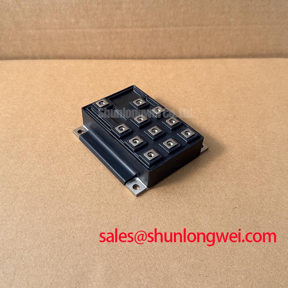
Two prominent examples of modern modular power engineering are the Fuji 6MBI100FC-060 and the Fuji 2MBI200U4H-120. While both devices stem from Fuji Electric's established power semiconductor lines, they are engineered for distinctly different topologies, voltage tiers, and power ratings. The 6MBI100FC-060 is a 6-pack (six-in-one) module rated for 600V and 100A, integrating an entire three-phase inverter bridge into a single, compact mechanical housing. It addresses the industry requirement for high power density and simplified board layout in 200V to 400V AC class industrial motor drives operating in the 15 kW to 30 kW range. In contrast, the 2MBI200U4H-120 is a half-bridge (dual-pack) module rated for 1200V and 200A, utilizing Fuji's advanced U4 trench-gate technology. By delivering higher breakdown voltage and handling double the continuous current in a two-switch phase-leg configuration, the 2MBI200U4H-120 solves the severe thermal and mechanical stresses encountered in heavy-duty 400V to 480V utility-connected industrial equipment, large regenerative drives, and commercial power converters.
2. Internal Physics and Operational Mechanics of IGBT Devices
To evaluate how modules such as the 6MBI100FC-060 and 2MBI200U4H-120 perform under operating conditions, an engineer must first understand the internal physical mechanisms governing IGBT conduction and commutation. A discrete IGBT chip is physically constructed as a multi-layer semiconductor device combining alternating p-type and n-type silicon layers: an n-channel MOS gate structure positioned above an n- drift region, which sits atop an injection p+ collector layer.
Figure 1: Internal Cross-Sectional Structure and Operational Equivalent Circuit of an IGBT Die
When the module is in its forward blocking state, the collector terminal is held at a positive potential relative to the emitter terminal, but the gate-to-emitter voltage (VGE) remains at 0V or is biased slightly negative (such as -5V to -15V). In this condition, the internal p-n junction between the p-base and the n- drift layer is reverse-biased, supporting the full bus voltage and preventing current flow except for a minute leakage current. When a positive control voltage exceeding the gate threshold voltage (VGE(th), typically between 5.5V and 7.5V) is applied across the gate and emitter terminals, an electric field forms across the thin gate dielectric oxide. This field repels holes and attracts free electrons to the silicon surface beneath the gate, creating an n-type inversion channel through the p-base region.
Once this channel forms, electrons flow from the emitter contact through the inversion channel into the thick, lightly doped n- drift layer. This influx of electrons acts as base drive current for the wide-base PNP bipolar transistor structure formed by the p+ collector substrate, the n- drift layer, and the p-base. In response, the p+ collector injects an abundance of positive holes into the n- drift layer. This phenomenon is termed conductivity modulation. Under conductivity modulation, the concentration of injected charge carriers (both electrons and holes) vastly exceeds the baseline background doping concentration of the drift region. Consequently, the apparent electrical resistance of the drift layer drops by orders of magnitude compared to an unmodulated drift layer of identical thickness in a high-voltage MOSFET.
Because of conductivity modulation, the on-state saturation voltage drop (VCE(sat)) between collector and emitter remains remarkably low—typically between 1.7V and 2.3V—even while conducting dozens or hundreds of amperes. However, this advantage involves an engineering trade-off during turn-off. When the gate drive removes the positive bias and grounds or reverses the gate voltage, the MOS inversion channel immediately closes, cutting off the supply of electrons. However, the holes that were injected into the wide n- drift region cannot vanish instantaneously; they must either be extracted by the electric field or disappear through natural recombination. This delayed evacuation of excess carriers manifests externally as a "turn-off tail current."
During the duration of this tail current, full collector-to-emitter voltage is already re-established across the terminal, resulting in simultaneous high voltage and declining current. This intersection produces turn-off switching energy loss (Eoff). Advanced manufacturing technologies address this behavior. The 6MBI100FC-060 utilizes planar punch-through design optimized for robust short-circuit ride-through, while the 2MBI200U4H-120 incorporates Fuji's U4 trench-gate technology paired with a field-stop buffer layer. The trench-gate architecture etches vertical channels directly into the silicon, yielding a vertical MOS channel that increases cell density and eliminates parasitic JFET resistance. Concurrently, the thin drift region terminated by a field-stop buffer sharply reduces the volume of stored minority charge, cutting turn-off tail times to fractions of a microsecond and drastically lowering overall switching dissipation.
3. Key Features, Advantages, and Technology Comparison
Selecting between different power modules requires evaluating their silicon technology, internal topologies, switching dynamics, and thermal structures. The Fuji 6MBI100FC-060 and Fuji 2MBI200U4H-120 represent two distinct operational philosophies within industrial power design.
The 6MBI100FC-060 integrates six active IGBT switches and six matched fast-recovery antiparallel diodes in a compact, unified package (often designated as an Econopack or similar standard multi-pack outline). This six-in-one topology is engineered explicitly to form the entire three-phase AC inverter bridge from a single assembly. By housing all six switches internally, the module eliminates external busbar interconnections between phases, drastically reducing total stray loop inductance between the upper and lower arms. This architecture is especially suited for compact variable frequency drives (VFDs) running on 200V to 240V utility supplies, or 380V lines where DC link voltages remain below 500V. Engineers can also explore complementary half-bridge systems or rectifier topologies such as the SKD75GAL123D to understand how dedicated power stages handle rectifier-inverter duties.
Conversely, the 2MBI200U4H-120 provides a dual-switch phase-leg (half-bridge) configuration rated for 1200V and 200A. Constructed with Fuji's U4 generation trench-gate technology, it achieves a nominal VCE(sat) of approximately 1.95V to 2.35V despite its high 1200V breakdown threshold. Because an entire three-phase bridge requires three separate 2MBI200U4H-120 modules, the system designer distributes the total generated thermal power over three discrete mechanical baseplates rather than concentrating it onto one. This distributed layout enhances heat extraction across large air-cooled or liquid-cooled heatsinks and allows the use of wide, planar copper laminated busbars that carry up to hundreds of amperes of continuous ripple current. This modular strategy is conceptually similar to deploying heavy industrial switches like the QM300HA-H, which served earlier generations of high-capacity motor controls, or modern compact converter units such as the DP15H1200TO101982 used in specialized equipment.
| Engineering Metric / Specification | Fuji 6MBI100FC-060 | Fuji 2MBI200U4H-120 | Engineering Significance & Impact |
|---|---|---|---|
| Internal Circuit Topology | Six-Pack (Three-Phase Bridge) | Dual Pack (Half-Bridge / Phase Leg) | Determines physical layout: unified compact bridge vs. modular distributed bridge design. |
| Collector-Emitter Voltage (VCES) | 600 V | 1200 V | Defines maximum allowable DC bus voltage; 600V modules suit 200-400V buses, 1200V suit 600-800V buses. |
| Continuous Collector Current (IC at TC=80°C) | 100 A | 200 A | Dictates steady-state load handling and maximum continuous motor power output. |
| Pulsed Collector Current (ICRM, 1 ms) | 200 A | 400 A | Governs peak overload, motor starting inrush current, and dynamic acceleration limits. |
| Saturation Voltage (VCE(sat), typical) | 2.00 V (at 100A, 25°C) | 1.95 V (at 200A, 25°C) | Directly establishes continuous conduction losses; lower values enhance overall conversion efficiency. |
| FWD Forward Voltage (VF, typical) | 2.20 V | 1.90 V | Determines freewheeling diode power dissipation during inductive load freewheeling cycles. |
| Thermal Resistance, Junction-to-Case (Rth(j-c)) | 0.35 °C/W (per IGBT) | 0.14 °C/W (per IGBT) | Indicates heat transfer efficiency; lower thermal resistance enables higher continuous power extraction. |
| Gate-Emitter Threshold Voltage (VGE(th)) | 5.5 V to 8.5 V | 6.0 V to 8.0 V | Sets minimum voltage required for turn-on; ensures reliable noise margin against false triggering. |
| Input Capacitance (Cies, typical) | 11.0 nF | 32.0 nF | Directly impacts gate driver sizing, peak drive current requirements, and gate charge time. |
| Recommended Switching Frequency Range | 2 kHz to 15 kHz | 2 kHz to 20 kHz | Higher switching capability allows acoustic motor noise reduction and smaller passive filter footprints. |
The performance differences summarized above emphasize that the 6MBI100FC-060 is optimized for volumetric compactness and low design complexity in standard low-voltage installations, whereas the 2MBI200U4H-120 is built to withstand higher electrical and thermal demands in medium-voltage industrial environments.
4. Real-World Applications and Operating Precautions
IGBT modules operate in harsh electrical and mechanical environments where poor implementation can cause rapid failure. The Fuji 6MBI100FC-060 is widely deployed in commercial HVAC multi-split inverter compressors, factory automation servo drives, motorized material handling conveyors, and small-to-midsize industrial pumps. In these installations, the motor is typically powered by a rectified 200V to 240V three-phase grid, or a lightly loaded 380V line equipped with comprehensive dynamic braking. Here, integrating all switching elements into a single module helps engineers design compact enclosures that fit directly onto the motor housing.
Figure 2: Three-Phase Inverter Topography Illustrating Parasitic Inductances and Gate Protection
The Fuji 2MBI200U4H-120 serves significantly larger, more demanding infrastructure. Its 1200V rating makes it an industry-standard choice for three-phase motor drives connected to 400V, 460V, or 480V utility mains, where the rectified DC bus routinely reaches 560V to 750V, with dynamic braking thresholds extending to 800V. It is equally common in central utility solar inverters, large uninterruptible power supplies (UPS) protecting data centers, regenerative lift cranes, and high-frequency induction heating power supplies. Further system-level context on how these modules interface with line filters and power grids can be found in discussions of Power Electronics Principles.
Thermal Interface and Mounting Practices
Because an IGBT die may generate power loss densities exceeding 100 W/cm2 during peak operation, proper mechanical installation onto a heatsink is essential. Thermal transfer failure is a leading cause of premature module destruction. Technicians and assembly engineers must follow these physical assembly guidelines:
- Heatsink Flatness and Surface Roughness: The contact surface of the aluminum heatsink must have a surface flatness error of less than 50 µm over a 100 mm span, and a surface roughness (Rz) of less than 10 µm. Protrusions, burrs, or scratches prevent true planar contact and create localized air pockets that act as thermal barriers.
- Thermal Interface Material (TIM) Application: A high-performance thermal grease with a bulk thermal conductivity of at least 1.5 to 3.0 W/(m·K) must be applied evenly across the baseplate. The layer must be controlled to an optimum thickness between 50 µm and 100 µm. Applying insufficient grease leaves micro-voids, while excessive grease increases thermal impedance and can cause the baseplate to bend when torqued down.
- Sequential Screw Tightening: Fastening screws must be torqued in a defined, two-stage cross pattern. For both the 6MBI100FC-060 and the 2MBI200U4H-120, screws must first be tightened to a temporary pre-torque of approximately 0.5 N·m to evenly distribute the thermal paste. Following pre-tightening, a final torque of 2.5 N·m to 3.5 N·m (conforming to M5 screw specifications) should be applied in an identical diagonal sequence. Uneven tightening bows the internal DBC ceramic, causing microscopic fractures that compromise dielectric isolation.
Electrical Gate-Drive and Parasitic Inductance Considerations
Fast switching of large currents induces transient voltages governed by the basic circuit relation V = -L · (di/dt). When turning off 200A in 0.2 µs, a parasitic busbar inductance of just 30 nH will generate an inductive voltage surge of 30V above the steady-state DC bus voltage. If the DC link voltage is 750V, this transient can easily breach the absolute maximum breakdown rating of the module, triggering avalanche breakdown and device destruction.
To prevent this, high-frequency polypropylene film snubber capacitors must be installed as close as physically possible directly across the DC positive and negative bus terminals of each module. Furthermore, gate-drive circuits must incorporate an active Miller clamp or a negative gate bias (such as -8V or -15V) during the off-state. When high-voltage transitions (dV/dt) occur across the collector-emitter terminals of the opposite switch in the half-bridge leg, displacement current flows through the internal Miller capacitance (Cres) into the gate node. If the gate impedance is too high or held purely at 0V, this displacement current can elevate the gate voltage above VGE(th), causing a "shoot-through" condition where both upper and lower switches conduct simultaneously, effectively short-circuiting the DC bus.
Electrostatic Discharge (ESD) Measures
The gate structure of an IGBT consists of an extremely thin silicon dioxide layer (typically under 100 nm thick). Any electrostatic potential exceeding ±20V can rupture this dielectric layer, causing permanent gate leakage or complete short-circuits. Assembly staff must wear grounded wrist straps, work on dissipative conductive surfaces, and keep the factory-supplied conductive terminal shunts in place on the gate pins until the module is securely soldered or connected to its dedicated gate driver board.
5. Engineering Selection Guidelines and Field Diagnostics
Specifying the proper power module requires balancing electrical safety margins, thermal limits, and real-world system losses. Below are systematic selection criteria for evaluating the 6MBI100FC-060 and 2MBI200U4H-120 against specific power stage requirements.
Voltage and Current Derating Rules
A reliable power engineering rule of thumb dictates operating an IGBT module at no more than 60% to 70% of its absolute maximum rated collector-emitter breakdown voltage (VCES) under steady-state DC bus conditions. The remaining 30% to 40% margin is necessary to absorb high-voltage transients created by grid surges, inductive load kickback, and parasitic busbar turn-off spikes. Consequently, the 600V-rated 6MBI100FC-060 is appropriately paired with a nominal DC bus voltage of 300V to 400V (such as derived from a 230V AC utility supply). In contrast, the 1200V-rated 2MBI200U4H-120 is engineered to handle 600V to 800V DC links (derived from 400V to 480V AC utility mains).
Current ratings must be calculated based on junction temperature (Tj) limits rather than simple catalog continuous ratings (IC). Although the 2MBI200U4H-120 is rated for 200A at a case temperature (Tc) of 80°C, the actual usable continuous current depends heavily on the switching frequency (fsw), the duty cycle, and the thermal resistance of the heatsink system. As the switching frequency increases from 4 kHz to 15 kHz, switching losses (Eon + Eoff) quickly overtake steady-state conduction losses (IC · VCE(sat)). Engineers must calculate total power dissipation using the relationship:
Ptotal = Pconduction + Pswitching = [D · VCE(sat) · IC] + [fsw · (Eon + Eoff)]
The resulting maximum silicon junction temperature must always remain below the 150°C maximum limit, with standard industrial designs derating this value to a maximum operating Tj of 125°C to ensure long-term thermal cycling reliability.
Bench and Field Diagnostic Procedures
When an inverter or motor drive faults out with an overcurrent, ground fault, or desaturation trip, the power module must be verified before replacing gate drivers or reconnecting line power. Technicians can perform reliable field diagnostics using a standard Digital Multimeter (DMM) set to Diode Test mode and High-Resistance (Ω) mode. Before testing, all DC bus capacitors must be discharged to 0V and verified with a voltmeter, and all external motor cables and gate drive harnesses must be disconnected from the module terminals.
| Test Configuration | Positive DMM Lead (+) | Negative DMM Lead (-) | Normal Expected Value | Failure Reading & Internal Defect Mode |
|---|---|---|---|---|
| FWD Diode Health (Upper Arm) | Module Emitter (E) / Output Phase (U/V/W) | Module Collector (C) / DC Bus (+) | 0.300 V to 0.450 V (Diode Mode) | 0.000 V (Short-circuited FWD die) or Over-Range "OL" (Open-circuited bonding wires) |
| FWD Diode Health (Lower Arm) | DC Bus (-) | Module Output Phase (U/V/W) | 0.300 V to 0.450 V (Diode Mode) | 0.000 V (Punctured junction) or "OL" (Blown bond wire from severe overcurrent) |
| IGBT Forward Blocking Check | Module Collector (C) / DC Bus (+) | Module Output Phase or Emitter (E) | Over-Range "OL" (High-Z state) | Near 0.000 V (Collector-Emitter punch-through or catastrophic thermal latch-up) |
| Gate Oxide Dielectric Integrity | Gate Terminal (G) | Emitter Terminal (E) | Over-Range "OL" (Resistance > 10 MΩ) | Low resistance reading < 100 kΩ or short circuit (Gate oxide puncture from ESD or Miller transient) |
| Baseplate Galvanic Isolation | Any Power Terminal (C, E, Phase) | Metal Mounting Baseplate | Over-Range "OL" (Megohmmeter: > 100 MΩ at 1 kV) | Low resistance or continuity (DBC ceramic isolation substrate cracked or arc-faulted) |
For additional perspective on modern power semiconductors and their evolving silicon boundaries, technical designers can consult Industrial Power Semiconductor Solutions. By aligning practical bench measurements with verified design boundaries, engineers can systematically isolate root causes, protect downstream machinery, and maximize system uptime across demanding industrial installations.