Content last revised on October 12, 2026
Assembly Integrity & Layout Architecture: Implementing Planar Symmetrical Busbar Geometry for 6MBI15S-120
Planar busbar symmetry is the first layout issue to address when this Fuji Electric 6MBI15S-120, 1200 V, 15 A IGBT module is installed in a compact industrial inverter or high-speed CNC spindle drive. The commutation path should place the high-current supply and return conductors close together, with the switching loop kept short and mechanically stable. This reduces stray inductance, limits ringing, and helps the gate-drive waveform remain representative of the intended switching command.
A useful engineering relationship is that the switching-node peak voltage rises with DC-link voltage, commutation-loop inductance, and current slew rate. In practical commissioning, this means that an overshoot observed at the collector-emitter terminals cannot be judged from the module voltage rating alone. Measure the voltage directly at the power terminals with a suitable differential probe, use a short probe connection, and compare the result at the actual operating current and switching condition.
A planar arrangement with closely coupled positive and negative conductors is a suitable design consideration when the project requires very low commutation inductance. A target such as less than 25 nH may be used by a system designer as a project-specific layout objective, but it is not an official electrical rating of the 6MBI15S-120. The final geometry should be verified through switching tests, including the effect of copper thickness, terminal overlap, fastener pressure, insulating films, and the location of the DC-link capacitors.
Snubber selection should follow the measured ringing frequency and energy rather than a generic capacitor value. Start by identifying whether the dominant oscillation is caused by the power loop, the capacitor connection, the gate loop, or measurement technique. A snubber placed close to the switching path can reduce peak stress, but excessive capacitance may increase switching losses. The system engineer should therefore evaluate capacitor pulse-current capability, resistor heating, insulation spacing, and the resulting thermal load on the module.
For a compact CNC spindle drive, the mechanical stack-up deserves the same attention as the copper layout. The baseplate must sit evenly against the heatsink, the thermal interface must cover the intended contact area without contamination, and the clamping sequence should avoid twisting the module body. Check the fan path for dust accumulation and confirm that cable routing does not press against the gate terminals or introduce movement into the power connections.
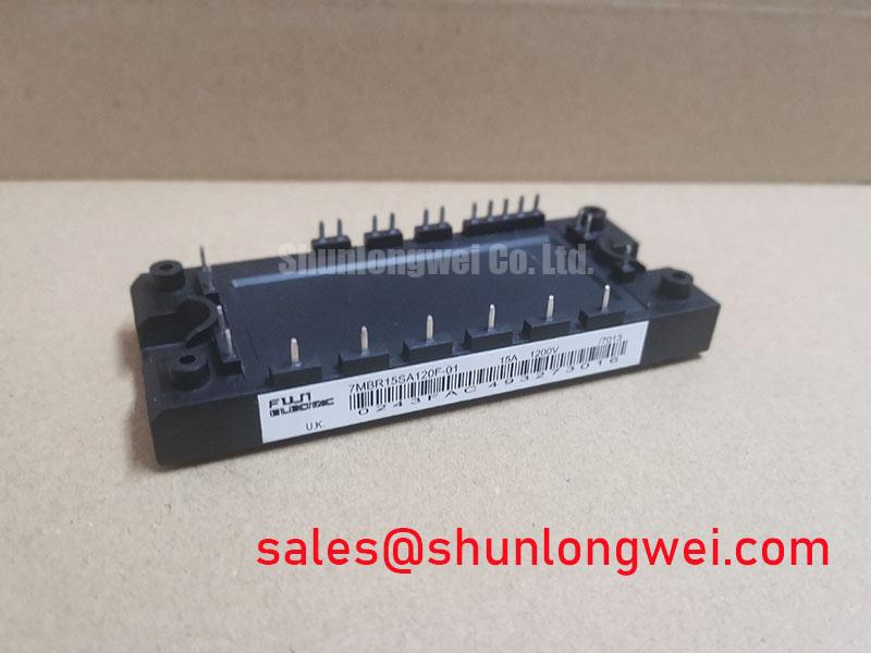
The module is a six-IGBT power module with a specified voltage rating of 1200 V and a rated collector current of 15 A under the datasheet-specified conditions. These values identify the component class, but they do not define the complete permissible operating area for every inverter topology. Switching frequency, duty cycle, cooling conditions, overload profile, gate-drive behavior, and transient voltage must be evaluated as a complete system.
Field Diagnostics & Commissioning: Oscilloscope Waveform Verification in 6MBI15S-120 Topologies
When retrofitting a legacy drive board, tune the external turn-on and turn-off gate paths from measured waveforms rather than from the resistor value fitted to the removed device. The practical objective is to control the compromise between switching loss, current slew rate, collector-emitter ringing, and gate-voltage stability. Separate turn-on and turn-off resistance can be useful during bench tuning, provided the driver output capability and protection behavior remain within the control board design limits.
Use suitably rated isolated or differential probes for both collector-emitter and gate-emitter measurements, with short, low-inductance connections. The probes must accommodate the actual common-mode voltage and switching transients; do not connect an earth-referenced oscilloscope ground to a floating emitter. Observe the gate plateau, the turn-off transition, the return to the off-state level, and any repeated oscillation after the current commutates. A waveform that appears clean at low bus voltage may behave differently at operating voltage because parasitic inductance and diode recovery interact with the actual load current.
Desaturation protection should be coordinated with the gate driver, fault latch, blanking interval, and soft turn-off path. A protection controller may use a response target below 3 µs in a particular system, but that timing is an engineering design requirement rather than an official rating stated for this module. The commissioning test should confirm that the protection circuit recognizes a short-circuit or abnormal collector-emitter rise quickly enough for the application, while avoiding nuisance trips during normal switching transients.
Two-stage soft turn-off can be evaluated where the driver architecture supports it. The first stage limits the immediate gate-drive transition, while the second stage completes the turn-off under controlled conditions. The correct timing and gate-current profile depend on the driver, wiring inductance, DC-link condition, and short-circuit energy. Validate the actual collector-emitter peak, gate-emitter excursion, and driver fault response with the module installed in its final mechanical arrangement.
Power-factor and front-end behavior also affect commissioning. In a phase-controlled rectifier, the conduction angle influences displacement power factor and harmonic current components. A compact inverter should be checked for the interaction between the rectifier, DC-link capacitor, line impedance, and any harmonic-reduction measures. The 6MBI15S-120 is the switching module in this discussion; it should not be presented as independently providing whole-equipment EMC or harmonic compliance. System-level measurements remain necessary.
| Item | 6MBI15S-120 | 2MBI200S-120-52 |
|---|---|---|
| Manufacturer | Fuji Electric | Fuji Electric |
| Specified voltage rating | 1200 V | Product documentation should be checked for the applicable rating |
| Rated collector current | 15 A under the datasheet-specified conditions | Product documentation should be checked for the applicable rating and conditions |
| Module configuration | Six-IGBT module | Dual-IGBT module |
| Replacement assessment | Reference device for the stated electrical boundary | Different circuit configuration; not a direct replacement |
The 2MBI200S-120-52 can be reviewed as a cross-model comparison, but its dual-IGBT configuration differs from the six-IGBT 6MBI15S-120. It is not a direct replacement. Any system redesign must account for pin arrangement, thermal interface, gate characteristics, electrical ratings, and dynamic behavior. A similar voltage class does not by itself establish interchangeability.
For an actively switched front end or related power stage, engineers may also review the 2MBI300VW-120D-51 as a separate system-level reference. This IGBT module is not a direct substitute for a diode or thyristor rectifier. It should be treated as a component for topology review, not as an automatic companion or replacement for the 6MBI15S-120.
Fuji Electric information on High-Speed Discrete IGBTs and SiC Devices provides useful background when comparing switching technologies. The comparison should remain tied to the actual gate driver, switching frequency, thermal design, and protection strategy of the equipment.
Benchtop Waveform Tuning: Mitigating Stress via Cold-State Main Terminal Impedance on 6MBI15S-120
Cold-state screening should be completed with the module disconnected from the DC link, gate driver, motor cable, and braking network, after verifying that stored energy has been safely discharged. Hold each gate at its corresponding emitter potential during main-terminal checks to prevent accidental turn-on from gate charge. Use the digital multimeter diode-check function across the main terminals and the antiparallel diode path, recording polarity and relative forward indication rather than treating one meter reading as a universal acceptance threshold. An unexpected difference between equivalent diode paths, an unexpected bidirectional conduction path, or a reading that changes sharply after repeated probing warrants comparison with a known-good device and an inspection of the surrounding circuit.
Gate leakage is checked separately with the gate terminals isolated from the driver and any temporary gate-emitter short removed. The test should confirm that the gate is not unintentionally coupled to the emitter or collector through wiring, contamination, a damaged driver output, or an incorrectly fitted snubber. Avoid charging the gate with uncontrolled bench equipment. The purpose of this stage is to identify abnormal terminal behavior before DC energization, not to simulate the full dynamic operating condition.
After the passive checks, connect the module to the gate driver with the power stage still unenergized. Observe the gate command, driver supply behavior, dead-time interaction, and fault feedback. This sequence helps separate a gate-loop problem from a main-terminal problem. If the gate waveform has excessive ringing, inspect the physical return path and driver reference before changing the external gate resistance.
Miller plateau behavior is especially important during waveform tuning. The effective capacitance associated with the collector-gate transition changes with voltage, and the charge drawn during the plateau influences the required driver current and switching duration. A driver that was adequate for a slower legacy device may show delayed turn-off, excessive gate disturbance, or protection timing errors after a retrofit. Adjustments should be made while monitoring both gate-emitter voltage and collector-emitter behavior.
Active collector-emitter voltage clamping may be considered when the switching loop produces a transient that threatens the collector-emitter voltage margin. Its operation must be coordinated with the external gate network and the driver’s fault response. The clamp voltage, current path, and energy handling are system design matters; they should be validated during controlled switching tests rather than inferred from the 1200 V module label.
Thermal recovery checks should include the heatsink contact, fan airflow, thermal interface condition, and temperature rise at the actual load profile. Repeated overload or surge events can produce junction-temperature peaks that are not apparent from external case-temperature measurements alone. The allowable surge current and recovery window must come from the applicable device documentation and the system’s thermal model, not from a generic IGBT rule.
⚠️ Maintenance Note: Inspect the heatsink airflow and thermal interface during scheduled service, and investigate any rising contact temperature before terminal discoloration or intermittent drive faults appear.
For long-running industrial equipment, maintenance records should pair terminal torque checks, cooling-path inspection, gate-driver fault history, and measured switching waveforms. The Industrial Applications reference can support broader topology discussions, while the actual acceptance decision for a 6MBI15S-120 installation remains tied to the inverter’s measured electrical, thermal, and mechanical conditions.