Content last revised on October 29, 2026
Preventing Spurious Faults: Negative Gate Bias vs Active Miller Clamping Guidelines for 2MBI900VXA-120E-50
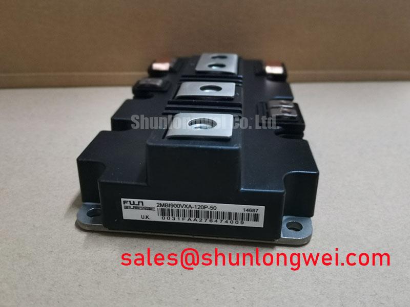
When a traction inverter reports an intermittent overcurrent event, check the gate-drive supply and inspect the turn-off waveform before replacing the power stage. The device identified for this service is the Fuji Electric 2MBI900VXA-120E-50, specified at 1200.0 V and 900.0 A in a Fuji Power Module package. These are product ratings; they do not by themselves define the allowable switching frequency, junction temperature, short-circuit duration, or complete inverter operating envelope.
High dv/dt at the switching node can couple current through the Miller capacitance of an IGBT and raise the gate potential during the intended off-state. A dedicated active Miller clamp provides a low-impedance path close to the gate-emitter loop, while a negative gate bias can add off-state immunity when the driver, isolation barrier, and module gate-emitter limits have been qualified together. The proposed negative-bias range of −5 V to −15 V should be treated only as a system-level design consideration, not as an official rating of this module. The final value must be established from the driver documentation, gate-emitter withstand data, switching overshoot, and measured gate-emitter transients.
For field diagnosis, probe the gate and emitter at the module terminals rather than at the driver board connector, using a differential or isolated probe rated for the common-mode voltage and transients. A long probe lead can introduce pickup that appears as a gate pulse. Compare the commanded gate signal with the actual gate-emitter waveform during both high-side and low-side transitions. An unexpected positive excursion during turn-off may indicate parasitic coupling, excessive common-emitter inductance, an incorrectly referenced emitter return, or excessive driver sink impedance. Check each possibility against a known-good phase leg instead of assigning a single cause from the fault code alone.
The gate loop should remain physically separate from the high-current commutation path. Keep the driver return routed directly to the intended emitter reference, minimize loop area, and avoid routing the gate trace alongside the collector or switching-node copper. When active Miller clamping is used, confirm that the clamp engages after the turn-off command without delaying the intended gate discharge. The gate resistor network should also be checked for cracked solder joints, incorrect split-resistor diode orientation, and unwanted impedance introduced by test points or adapter wiring.
Fuji Electric application material on IGBT brake chopper modules provides useful context for evaluating switching-device behavior in high-energy power conversion circuits. For a related discussion of Miller-induced parasitic turn-on mechanisms, see Mitigating Parasitic Turn-On in SiC MOSFETs; the device technology differs, but the gate-loop and common-mode measurement principles remain relevant.
2MBI900VXA-120E-50 Circuit Protection & Reliability: Calibrating a Retrofit: Tuning Turn-On/Turn-Off
Retrofitting a power module into a legacy drive board requires evaluating and, where necessary, recalibrating the external gate network rather than treating the replacement as a passive mechanical exchange. The 1200.0 V voltage class and 900.0 A current rating identify the component category, while actual switching stress depends on the DC link, commutation inductance, pulse duration, thermal path, gate-drive voltage, and protection response of the host inverter.
Separate turn-on and turn-off resistors can help balance switching loss against di/dt-related ringing. A lower turn-on impedance may shorten the transition but can increase current overshoot, electromagnetic emission, and diode reverse-recovery interaction. A higher turn-off impedance may reduce ringing in some layouts while increasing turn-off loss. These are engineering trade-offs, so the retrofit should be calibrated by observing collector-emitter voltage, collector current, gate-emitter voltage, and case temperature under controlled switching conditions.
When the legacy board has a single fixed gate resistor, inspect the driver’s peak source and sink current before adding a split network. The resistor must be placed close to the module gate terminal, with the emitter return kept adjacent to the gate path. Gate wiring shared by multiple parallel modules can create unequal dynamic drive conditions even when the schematic appears symmetrical. Each module should have an equivalent physical path, and the busbar geometry should distribute current without forcing one device to carry a disproportionate commutation loop.
Static current sharing in parallel IGBTs is influenced by the temperature behavior of VCE(sat), gate-drive matching, and thermal coupling; stray inductance and the timing relationship between devices also affect dynamic sharing. A positive temperature coefficient in the relevant operating region can support current balancing, but it should be confirmed from the applicable electrical characteristics rather than assumed across every load and temperature. The commissioning engineer should compare current sharing at startup, rated load, regenerative operation, and fault recovery.
Protection coordination is equally important. Desaturation detection, soft shutdown, gate undervoltage monitoring, overtemperature feedback, and DC-link overvoltage protection must be checked as one chain. A protection circuit that reacts correctly on a low-energy bench supply may behave differently when the traction inverter contains a long busbar, large braking energy, or a fast diode recovery event. The Fuji Electric RC-IGBT module information can also help engineers compare integrated reverse-conduction approaches, while the present module should remain evaluated against its own documented topology and terminal arrangement.
The 2MBI300UD-120-02 is a separate device for comparison; compatibility with the host inverter is not established here. It should not be treated as an automatic substitute for the 2MBI900VXA-120E-50. Any proposed substitution requires complete voltage, current, gate-drive, mechanical, thermal, and protection verification.
Preventing Spurious Faults: Common-Mode Transient Immunity in Harsh Industrial Environments for 2MBI900VXA-120E-50
Common-mode transient problems should be investigated at the isolation barrier and gate-driver reference before changing the IGBT gate resistance. In a high-speed rail or heavy freight locomotive traction inverter, the switching node can move rapidly relative to the control electronics, coupling displacement current through isolation capacitance, heatsink structures, cable shields, and measurement equipment. A false gate pulse may appear when the driver supply momentarily shifts, the isolated power supply rebounds, or the emitter reference is disturbed.
Reinforced galvanic isolation and common-mode transient immunity belong to the driver and isolation architecture, not automatically to the power module. Values such as isolation above 5 kV or CMTI above 100 kV/µs are system selection targets that must be supported by the chosen optocoupler, digital isolator, isolated power supply, and safety documentation. An isolation withstand voltage alone does not establish reinforced insulation or an allowable continuous working voltage. They are not official specifications supplied here for the Fuji module. The isolation coordination should also consider creepage, clearance, pollution level, transient overvoltage category, and the physical geometry of the assembled inverter.
During troubleshooting, monitor the isolated driver supply, input-side logic signal, output-side gate signal, and emitter reference with probes rated for the common-mode environment. Look for narrow pulses synchronized with the opposite switch transition, supply dips during gate charging, and ringing that crosses the driver’s input threshold. A driver with adequate nominal CMTI can still be compromised by poor PCB return routing, excessive isolation capacitance, or a gate loop that shares copper with the power commutation path.
Bootstrap-based high-side supplies require particular attention. The bootstrap capacitor must retain sufficient gate-drive energy during the intended high-side on-time, and its charging diode must tolerate the switching pattern and recovery behavior of the circuit. The capacitor, diode, series impedance, and high-side driver reference should be checked together during repetitive operation rather than only with a static voltage measurement. If the original board uses a bootstrap arrangement, verify its refresh interval and startup behavior before installing a replacement module with different switching characteristics.
EMI troubleshooting should separate conducted disturbances from radiated coupling. A temporary reduction in switching speed may help identify whether the fault is related to commutation edge energy, but the final setting must satisfy thermal loss, switching loss, and protection requirements. Shield termination, isolated supply layout, gate-return routing, and busbar symmetry should be validated under the actual cabinet configuration. The module itself should not be described as independently certified for complete-system EMC compliance.
Field Diagnostics & Commissioning: Baseplate Convexity Inspection in 2MBI900VXA-120E-50 Topologies
Before applying full load, inspect the mounting interface for baseplate convexity, heatsink flatness, contamination, and uneven contact marks. The purpose is to establish a continuous thermal path without mechanically loading the module substrate. A distorted heatsink or excessive local pressure can create thermal gradients and electrical stress even when the module terminals are correctly wired.
Use a calibrated straightedge, suitable feeler gauges, and a clean inspection surface to compare the heatsink across its length and diagonals. Do not infer flatness from the appearance of the thermal interface material. The mounting surface should be free of burrs, metal particles, old compound, and raised machining marks. If the baseplate or heatsink shows abnormal contact at only one edge, stop the installation and correct the mechanical interface before energizing the DC link.
Apply the thermal interface material as a thin, continuous layer appropriate for the selected compound and surface condition. Follow the applicable Fuji Electric mounting instructions and the compound manufacturer’s application method when selecting the layer thickness, taking actual surface flatness into account. Excess material can migrate toward terminals, while insufficient coverage can leave dry regions that increase thermal resistance.
Fasteners should be tightened progressively in the sequence specified by Fuji Electric so the module settles evenly against the heatsink. The correct torque must come from the Fuji mechanical documentation and the fastener assembly specification; do not substitute a generic torque value for the manufacturer’s instruction. After tightening, inspect for baseplate rocking, displaced compound, tilted terminals, and changes in heatsink contact. A thermal scan during a controlled load test can reveal uneven heat spreading, but it should be interpreted alongside electrical current sharing and coolant or airflow conditions.
💡 Pro Tip: Never connect or remove gate-drive wiring while the DC link or isolated driver supply is energized, even when the inverter control logic appears disabled.
For commissioning, begin with a controlled low-energy test that confirms gate polarity, interlock timing, dead-time behavior, and protection feedback. Increase power only after the measured gate-emitter waveform remains clean at the module terminals and the mechanical interface remains stable. Record collector-emitter overshoot, phase-current balance, heatsink temperature distribution, and fault response so later maintenance teams can compare the repaired inverter against its verified baseline.