Content last revised on October 21, 2026
Field Diagnostics & Commissioning: Cosmic-Ray Robustness and Voltage Derating in FF1200R12IE5P Topologies
- Isolate the DC link, verify discharge with an appropriate instrument, and disconnect parallel circuit paths before checking cold terminal impedance.
- Compare collector-to-emitter and gate-to-emitter measurements with the equipment schematic and a known-good assembly; record polarity and instrument settings.
- Inspect terminal seating, busbar alignment, mounting surfaces, and fasteners before disturbing the existing installation.
- Check driver supply integrity and the gate inhibit path before authorizing any energized commissioning test.
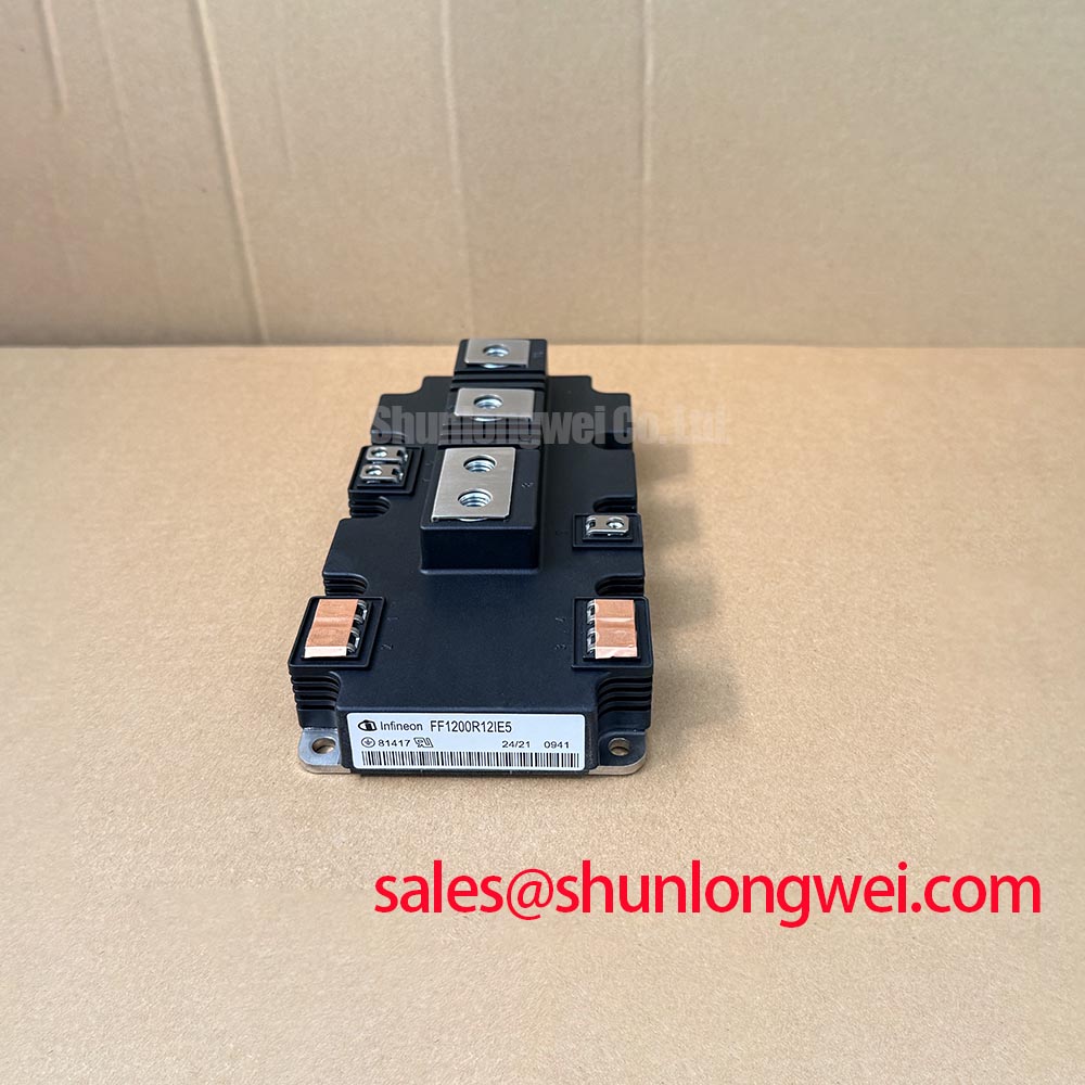
The FF1200R12IE5P is an Infineon IGBT Module with supplied official ratings of 1200 V and 1200 A. For repair assessment, establish its electrical identity first, then evaluate the surrounding power stage rather than treating the module as an isolated replacement. Cold measurements can identify suspicious differences, but they do not establish switching performance or remaining service life.
| Product characteristic | Value | Parameter identity |
|---|---|---|
| Manufacturer and model | Infineon FF1200R12IE5P | Product identification |
| Rated blocking voltage | 1200 V | Official Specification |
| Rated current | 1200 A | Official Specification; operating conditions govern application |
| Package category | Module | Official Specification |
| Terminal arrangement, mounting limits, and switching characteristics | Consult Datasheet | Required for installation approval |
Record the actual voltage across the blocked device during steady operation, startup, and shutdown before assessing voltage headroom. As a Design Consideration, distinguish sustained blocking stress from switching overshoot: reducing one does not automatically control the other. Measurements should capture the relevant device terminals using appropriately rated probes and a connection arrangement that does not introduce misleading ringing.
For elevated installations, include site altitude in the engineering assessment rather than assigning a universal derating threshold. Cosmic-ray-related semiconductor failure assessment requires applicable manufacturer characterization covering device technology, blocking voltage, and environmental assumptions. A defensible SEB or FIT calculation cannot be obtained from the 1200 V rating alone. Procurement and maintenance teams should request the applicable reliability assessment when this mechanism is part of the equipment acceptance criteria.
As a Design Consideration, investigate repeated failures against recorded bus conditions, protection events, cooling condition, and switching waveforms before attributing them to atmospheric radiation. A damaged module does not identify the initiating mechanism. Keep the failure history tied to the equipment configuration so that changes in bus regulation or driver hardware remain distinguishable from environmental effects.
For compatibility assessment, a utility-scale 1500 V central solar photovoltaic inverter requires particular care: a 1200 V device must not be assumed capable of blocking the full input bus. Evaluation belongs at the individual switching position in the actual multilevel or otherwise voltage-managed circuit, including abnormal operating states. The equipment schematic and measured device stress determine whether that position is suitable.
Maintain conductor spacing and insulation arrangements according to the equipment insulation-coordination requirements, accounting for the installation environment. The Infineon IGBT Modules & Discretes Official Portfolio provides manufacturer context for the device family; model-specific operating limits remain the basis for component approval.
FF1200R12IE5P Circuit Protection & Reliability: Torque Control and Transient Absorption
Seat the external busbar without pulling it into alignment through the module terminals. As a Design Consideration, check the complete fastening stack, including conductor thickness, washers, and usable thread engagement. A screw that reaches the bottom of a threaded connection can register torque without producing the intended clamping force, while an unsupported conductor can impose bending loads after tightening.
Use the applicable assembly instructions to establish fastener type, engagement, tightening method, and torque. Witness marks can support inspection, but they do not measure clamp load. Where vibration or thermal movement is relevant, inspect the external support arrangement and look for displaced hardware, fretting, or conductor movement without inferring the condition of inaccessible internal joints.
Field Alert: Do not use terminal screws to pull a misaligned busbar into position; correct the external alignment before tightening to the specified assembly procedure.
On the electrical side, diode reverse recovery and commutation-loop inductance can contribute to voltage overshoot and ringing. This is a Design Consideration, not a verified reverse-recovery characteristic of this particular module. Compare current transfer and collector-emitter voltage during controlled switching tests before changing a snubber. Evaluate any adjustment against peak voltage, dissipation, temperature, and the equipment’s emissions measurements.
A MOV-based absorption network should be assessed against its location and intended surge duty. Its clamping behavior, connecting inductance, and energy capability determine which disturbances it can address; it should not be treated as a universal substitute for local switching-transient control. Likewise, a snubber change is not evidence of system-level EMC compliance.
When reviewing other power-stage positions, the FS200R12PE4 can be examined as a separate component reference within the wider circuit assessment, not automatically assigned as a rectifier or complementary replacement. The schematic must establish each device’s function. A comparison with FZ1800R12KF4_S1 similarly requires circuit configuration, terminal mapping, mechanical fit, driver compatibility, and switching review; a verified direct replacement relationship is not established here.
FF1200R12IE5P Operational Boundaries: Preventing Ceramic Substrate Damage During Assembly
Inspect the heatsink contact surface and module mounting face for contamination, raised burrs, and damage before applying interface material. As a Design Consideration, assess flatness and any specified mounting-face profile using the manufacturer’s measurement method. Do not machine, lap, or straighten a module mounting face based on an assumed requirement for perfect flatness.
Prepare the thermal interface using the approved material and application process. Coverage, bond-line behavior, surface condition, and mounting pressure work together; an arbitrary paste thickness is not a validated instruction for the FF1200R12IE5P. Excess material does not correct a distorted heatsink, and uneven deposits can make repeatable assembly difficult.
Where the mounting procedure specifies staged tightening, follow its sequence with a calibrated tool rather than fully loading one corner first. The objective is controlled seating without imposing avoidable bending stress. This mechanical principle does not establish an internal substrate material or a model-specific fracture threshold. Inspect the accessible mounting condition instead of claiming an internal diagnosis from external appearance.
After assembly, compare temperature behavior under a controlled load with the equipment’s accepted baseline. Account for coolant or airflow conditions, sensor placement, and operating duty before interpreting a temperature difference. A local temperature increase may justify inspecting contact quality, current sharing, or cooling performance; it does not uniquely identify an interface defect.
For systems with repeated bidirectional power cycling, assess the operating profile and cooling regulation together. Reducing unnecessary temperature excursions is a Design Consideration, not a quantified life-extension promise. Record the conditions accompanying thermal observations so later maintenance decisions are based on comparable measurements.
Field Diagnostics & Commissioning: Driver Power Stage Start-Up and Inrush Mitigation in FF1200R12IE5P Topologies
Verify that the driver establishes its intended off state and valid undervoltage-lockout status before the equipment enables the DC link or switching commands. As an Engineering Recommendation, test startup, interrupted auxiliary power, and shutdown against the equipment’s approved sequence. Do not prescribe a negative gate-bias value independently of the module limits and driver design.
Separate auxiliary-supply inrush from unintended gate activation during the investigation. Check whether supply startup causes rail collapse, repeated resets, or inconsistent inhibit signals. Capture the gate-emitter waveform at the relevant terminals with suitable isolated measurement equipment, then correlate it with driver readiness and bus energization. An auxiliary rail that looks stable at its source can behave differently at the driver connection.
Assess dead time against actual turn-off behavior and propagation differences rather than copying a delay from another installation. As a Design Consideration, excessive overlap risks cross-conduction, while unnecessarily extended dead time changes commutation behavior and losses. The final timing belongs to the validated control and protection design.
Keep the gate drive and return paths compact to reduce parasitic inductance, and evaluate damping from measured switching behavior. Distinguish reverse-transfer capacitance from Miller charge when reviewing documentation; they are related switching quantities, not interchangeable labels. Any Miller clamp or active voltage-clamping function requires coordination with the driver, allowable gate stress, and fault response.
The Precision Gate Drive Design reference can support this review of gate-loop behavior and protection coordination. Before releasing the repaired assembly, verify that a loss of driver readiness inhibits switching and that shutdown does not leave an uncontrolled gate state while bus voltage remains present.