Content last revised on September 23, 2026
Preventing Spurious Faults: Optimizing Heatsink Contact Pressure and Mounting Guidelines for FZ1800R12KF4_S1
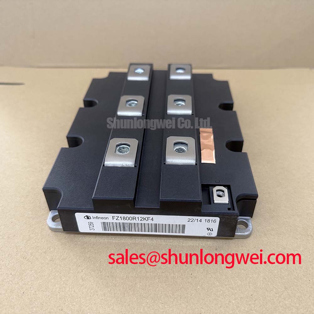
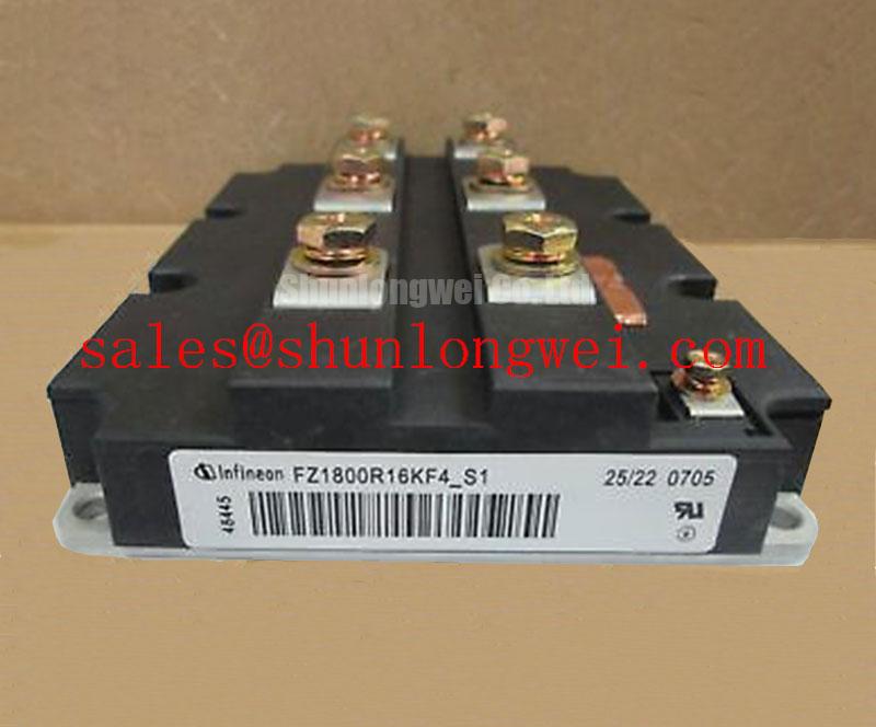
Start incoming inspection by confirming the FZ1800R12KF4_S1 marking, checking the documented terminal polarity, and using a multimeter diode range to compare the power terminals against a known-good reference under cold, isolated conditions. Do not infer a terminal function from physical position alone; verify it against the applicable Infineon mechanical and electrical documentation before applying any gate or collector voltage.
| Parameter | Official Specification |
|---|---|
| Manufacturer | Infineon |
| Collector-emitter voltage, VCES | 1200 V |
| Continuous collector current, IC at TC = 80°C | 1800 A |
| Short-circuit withstand time, tsc | 10 µs |
| Thermal resistance, junction-to-case per IGBT | ≤ 0.008 K/W |
| Maximum junction temperature, Tj,max | 150°C |
For a high-current module, the interface between the baseplate and heatsink should be treated as part of the thermal circuit rather than as a simple mechanical fastening point. A clean, flat heatsink surface and an even thermal interface layer help keep the measured case temperature representative of the actual mounting condition. Thermal interface material selection, thickness, and void control remain system-level design considerations because the correct values depend on the selected material, surface finish, flatness, and clamping method.
Install the module with the busbar and heatsink free from mechanical strain. Start all fasteners by hand, bring them into contact progressively, and use a diagonal tightening sequence so that the baseplate is not pulled unevenly against the cooler. The final mounting torque must come from the module drawing and the selected fastener specification rather than from a generic value. After assembly, inspect for rocking, visible gaps, displaced interface material, and busbar stress.
When a central solar photovoltaic inverter reports intermittent overtemperature or gate-driver faults, compare the temperature sensor location, heatsink flatness, mounting pattern, and phase-leg current balance before replacing the module. Clearance around the power terminals should also allow inspection and prevent accidental contact with adjacent conductors. A neutral reference for comparing a related high-current platform is FZ3600R12HP4, but mechanical and electrical interchangeability must be verified by the system engineer.
💡 Bench Tip: Use ESD protection and record cold-state diode-test observations before installation so later measurements can be compared with the original incoming baseline.
FZ1800R12KF4_S1 Circuit Protection & Reliability: Calibrating Transient Thermal Impedance
The published Rth(j-c) ≤ 0.008 K/W per IGBT value is a steady-state junction-to-case thermal specification. It should not be used alone to predict the peak junction temperature during a short overload or regenerative braking pulse. For pulsed operation, the design team should obtain the applicable transient thermal impedance curve and represent it with a validated multi-RC network. The resulting junction-temperature estimate must be checked against the 150°C maximum junction temperature under the actual pulse width, repetition rate, coolant condition, and current waveform.
In a regenerative braking chopper, the braking resistor and switching sequence determine how much energy is absorbed and how quickly it returns to the semiconductor. Verify the DC-link overvoltage response with the real resistor, wiring inductance, gate timing, and fault-clearance path. The module rating does not by itself confirm suitability for a particular braking duty. Designers should also coordinate semiconductor fast fuses and their I²t characteristics with the DC-link fault energy, while recognizing that fuse coordination cannot replace rapid gate shutdown and correctly rated buswork.
During incoming inspection, check the isolation condition between power terminals and the baseplate using the approved test method and voltage specified by the relevant documentation. Creepage and clearance must be evaluated in the complete inverter assembly, including contamination level, altitude, coatings, barriers, and busbar geometry. A measured insulation result should be compared with the approved production limit, not with an invented universal pass value.
Transient Dynamics & Electrical Design: High-Speed Fault Management: VCE Desaturation on FZ1800R12KF4_S1
The official 10 µs short-circuit withstand time is a protection boundary, not a target operating interval. The gate-driver architecture should detect abnormal VCE behavior promptly and complete a controlled shutdown within the verified protection budget. Type-I or type-II detection terminology may vary between driver platforms, so the selected desaturation circuit must be tested with the actual module, gate resistance, DC-link voltage, current path, and temperature range.
Two-stage soft turn-off can be evaluated where the system requires reduced di/dt during fault interruption. Its timing and gate-current profile must be validated on an oscilloscope because parasitic inductance can create a collector-emitter overshoot that is not visible from a low-bandwidth control signal. Keep the fault-detection loop short, separate high-current commutation paths from sensitive feedback wiring, and verify the peak VCE against the module voltage rating during switching tests.
Industrial inverter control boards should also be checked for optocoupler or digital-isolator common-mode transient immunity under the real switching waveform. A fault signal that arrives late, resets intermittently, or changes state during a high dv/dt event may indicate an isolation-layout or measurement problem; compare it with a known-good signal path before assigning the cause to the IGBT module.
FZ1800R12KF4_S1 Circuit Protection & Reliability: Calibrating Active Miller Clamp Implementation
An active Miller clamp can help limit unintended gate-voltage movement during the opposite switch transition, but its effectiveness depends on driver placement, return-path inductance, gate-loop impedance, and the common-emitter arrangement available in the module assembly. These are design considerations rather than confirmed internal features of the FZ1800R12KF4_S1. The system integrator should verify the actual terminal configuration and driver interface before selecting a clamp topology.
Do not assume that a negative off-state gate bias is required or permitted without the relevant gate-emitter limits and driver documentation. The linked technical reference Evolution of Negative Off-Bias Gate Drive Circuits provides useful background for evaluating that approach, while Infineon’s RCDC application note and IGBT discretes and co-pack diode information can support topology-level review.
At commissioning, observe both gate-emitter voltage and collector-emitter behavior at the module terminals. Check for cross-conduction, delayed fault feedback, unequal phase-leg switching, and ringing that changes with probe position. Minimize parasitic commutation-loop inductance and verify the final switching margins with the assembled inverter, since active-clamp performance cannot be confirmed from a bench gate waveform alone.