

Content last revised on October 21, 2026
FF1200R12IE5 Operational Boundaries: Pre-Installation Junction Health Check
- Isolate the converter and confirm that the DC link is fully discharged before any terminal measurement.
- Record cold, unpowered readings between the main power terminals and across the antiparallel diode path.
- Inspect the mounting surface, thermal interface, terminal hardware, and driver insulation before installation.
- Check the legacy gate drive return path against the replacement module’s documented terminal assignment.
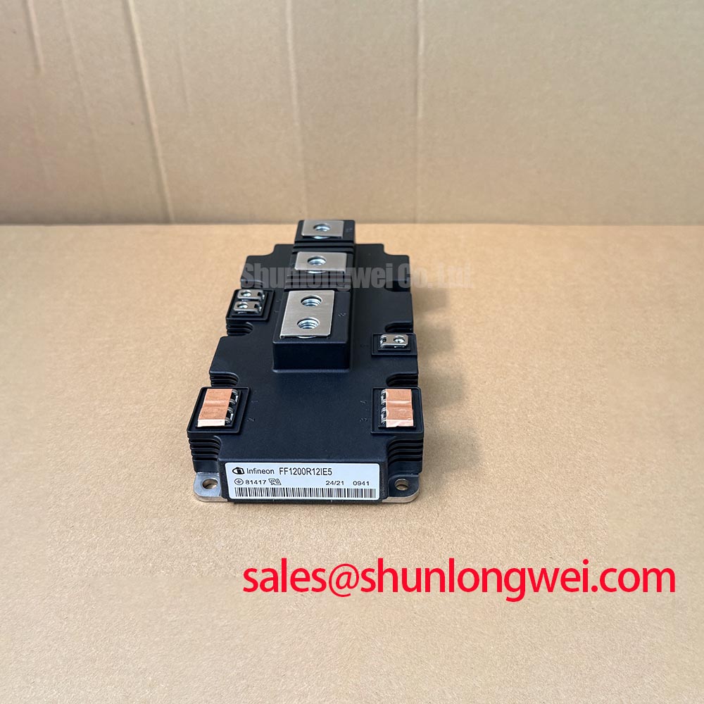
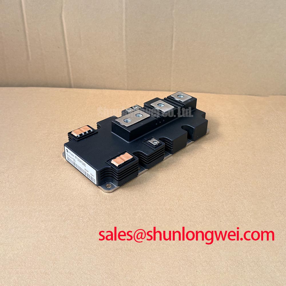
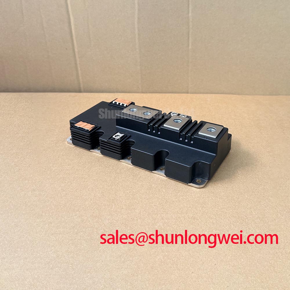
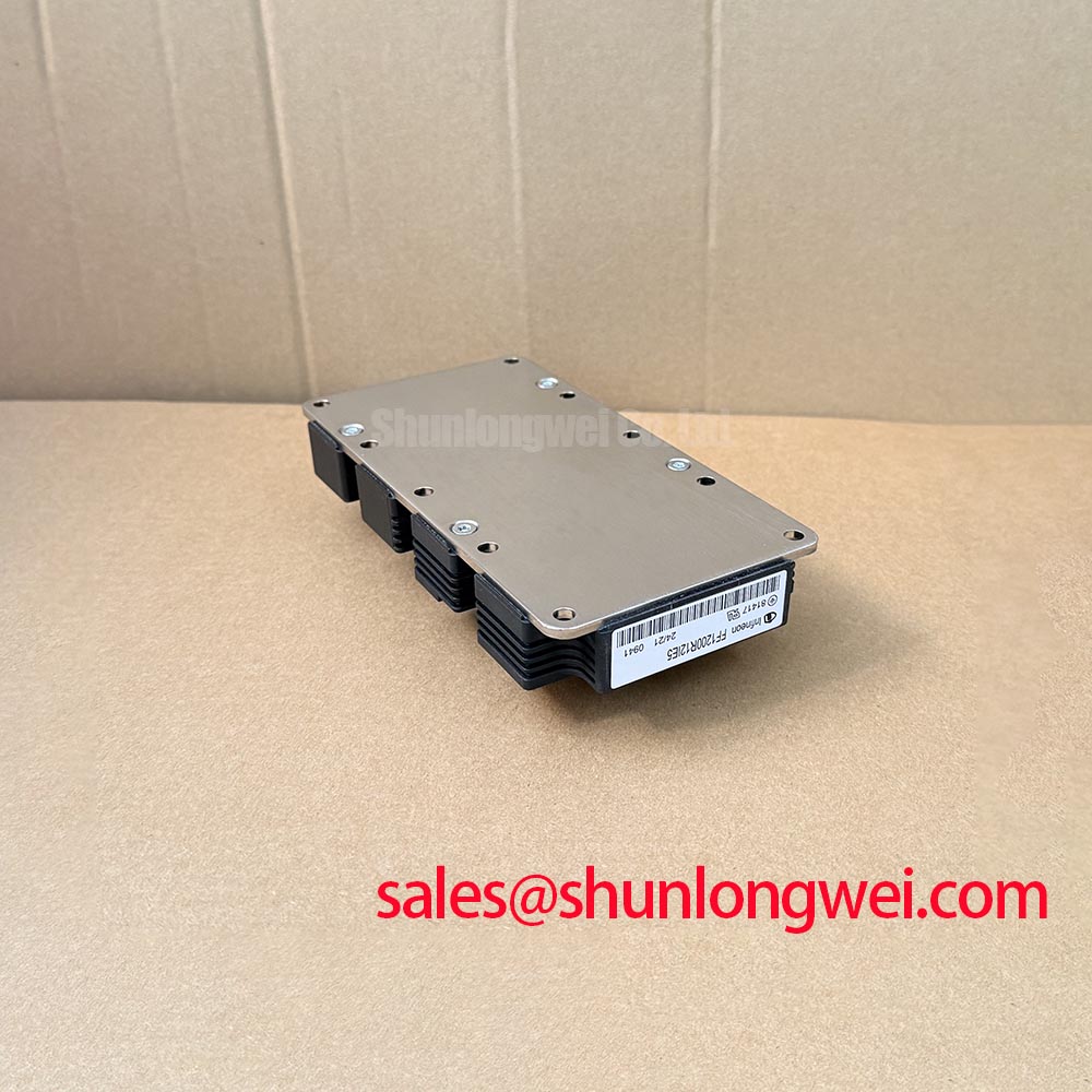
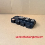
FF1200R12IE5 is an Infineon IGBT Module with a specified voltage rating of 1200 V and a rated collector current of 1200 A under the manufacturer’s specified conditions. The voltage and current ratings define the component category, but the complete operating point remains dependent on switching frequency, duty cycle, junction temperature, cooling system, gate drive behavior, and the converter topology.
| Parameter | Specification | Classification |
|---|---|---|
| Manufacturer | Infineon | Official product identification |
| Part number | FF1200R12IE5 | Official product identification |
| Rated voltage | 1200 V | Official Specification |
| Rated collector current | 1200 A, subject to datasheet conditions | Official Specification |
| Package | Module | Official Specification |
For a multi megawatt offshore or onshore wind turbine full scale converter, the module can be assessed within the power conversion stage only after the electrical, mechanical, thermal, and gate drive interfaces have been matched. The system integrator should compare the original converter documentation, wiring diagram, protection strategy, and cooling arrangement before energization. Infineon’s IGBT Modules and Discretes Official Portfolio and IGBT Modules Overview provide useful manufacturer level context for this component family.
Cold bench screening should start with the converter isolated, the DC link discharged, and the module disconnected from the gate driver. Hold each gate at its corresponding emitter potential during collector-emitter diode checks to prevent unintended turn-on from a floating gate. Use the digital multimeter diode check function across the main semiconductor terminals in both polarities, then repeat the measurement across the antiparallel diode path identified in the approved circuit documentation. The forward reading is a comparative screening value, not a substitute for a manufacturer test curve. Compare each reading with a known good device of the same type and with the expected polarity shown on the system schematic.
Gate leakage checks require the gate terminal to remain electrically separated from the external driver circuit during measurement. Confirm that the meter, test leads, and operator are not introducing uncontrolled charge into the gate circuit, and keep the test voltage within the specified gate limits. A stable open circuit indication or a low leakage condition by itself does not prove dynamic switching health, while an unexpected changing reading can justify further isolation of the gate resistor, driver output, and protection components. If the reading changes after handling, repeat the check with controlled grounding and clean terminal surfaces.
Use the cold check to identify inconsistencies before applying DC power. A conduction path that differs materially from the corresponding phase leg may indicate a damaged semiconductor path, contamination, an attached snubber, or an incorrect terminal assumption. Remove external parallel paths where practical and document the exact test points. The check should also include the freewheel diode direction because a healthy IGBT path and a healthy diode path are separate parts of the commutation behavior.
Physical clearance around the power terminals must support the converter’s insulation coordination, pollution environment, and enclosure design. Keep the gate driver wiring physically separated from high current commutation paths where the cabinet layout permits. For wind converter service work, salt contamination, condensation, vibration, and long cable runs deserve attention because they can change leakage and noise conditions without changing the module’s printed rating. These are design considerations, not additional factory specifications for this part.
Transient Dynamics & Electrical Design: Gate Drive Resistance Calibration for FF1200R12IE5 Replacement
Retrofitting FF1200R12IE5 onto a legacy drive board requires calibration of the external turn on and turn off gate resistance as a switching network, rather than treating either resistor as an isolated replacement value. Gate resistance affects current slew rate, switching loss, voltage overshoot, ringing, and the time spent on the Miller plateau. The correct balance is determined by the actual driver output impedance, gate charge behavior, commutation inductance, DC link condition, and thermal result in the assembled converter.
Begin with the existing driver topology and determine whether separate turn on and turn off paths are present. Confirm the gate clamp arrangement, desaturation or overcurrent response, and the route used for the emitter return. A legacy board may have been tuned around another module’s gate charge and internal inductance. Reusing the same resistor without checking the switching waveform can produce excessive ringing or an unnecessarily slow transition. The measurement should capture gate to emitter voltage, collector to emitter voltage, and phase current at the same switching event.
Parasitic inductance in the gate loop converts rapid changes in gate current into voltage disturbance. Keep the driver output, gate resistor, gate connection, and emitter return compact and closely coupled. The power commutation loop should remain physically distinct from the gate loop so that high di/dt current does not share the driver reference path. Miller effect can raise the gate voltage during the opposing device transition, so the protection method should be evaluated during both turn on and turn off events rather than during a static gate test.
Bench Diagnostic: Isolate control and power supplies and verify that the DC link is discharged before changing gate resistors or connecting measurement equipment. Verify the driver return and use appropriately rated, isolated or differential probes before the next pulse test.
Thermal installation must be checked at the same time as electrical tuning. The heatsink surface should be clean, flat, and free from particles, while the thermal interface material should form a continuous, controlled layer without voids or excessive squeeze out. Tighten the mounting hardware progressively in the sequence specified by the manufacturer so that the module base remains evenly seated. The final torque must follow the applicable module mechanical documentation and approved assembly procedure, not the electrical rating alone.
When a different topology or current class is being evaluated, the FF300R12KE3G may be reviewed as a separate Infineon module option, but its electrical and mechanical compatibility must be assessed independently. It should not be treated as an automatic substitute for this device.
Transient Dynamics & Electrical Design: Junction to Case Thermal Network Simulation on FF1200R12IE5
Thermal simulation should follow the real power pulse sequence rather than relying on a single steady state current figure. For FF1200R12IE5, the model should separate semiconductor conduction loss, switching loss, diode contribution, and the timing of repeated converter events. A multi stage RC network can represent junction to case transient behavior when the relevant thermal impedance data is available from the applicable technical documentation.
The practical workflow is to obtain the instantaneous loss profile from measured voltage and current waveforms, apply the pulse sequence to the thermal network, and compare the calculated junction temperature with the permitted operating boundary. The calculation should include the starting case temperature, heatsink response, cooling system condition, and neighboring module heating. A short overload pulse and a repeated overload train can produce different junction responses even when their average power is similar.
Thermal interface quality is part of the measurement chain. A simulation based on an ideal case temperature can hide mounting problems, uneven pressure, pump degradation, blocked airflow, or a contaminated cold plate. During commissioning, place temperature sensors at suitable case or heatsink locations and correlate them with the switching waveform and load record. The measured case response can then be used to refine the thermal network without claiming an unverified field lifetime.
For a wind turbine full scale converter, the cabinet operating profile may include low wind operation, rapid power changes, grid support events, and repeated thermal cycling. These conditions should be represented by the equipment duty record rather than by an assumed universal mission profile. The Wide Bandgap Revolution article offers broader background on switching technology and design challenges, while this module evaluation remains focused on the installed IGBT power stage.
Transient Dynamics & Electrical Design: Auxiliary Emitter Pinout Cold Check on FF1200R12IE5
The auxiliary emitter connection must be distinguished from the main load emitter path before the driver is connected. The auxiliary or Kelvin return, where provided by the applicable module construction, is intended to give the gate driver a cleaner reference than a high current load terminal. Do not infer the terminal assignment from physical position alone. Use the approved terminal drawing and board schematic, then trace continuity with the module unpowered.
A cold continuity check, together with the terminal drawing and board schematic, should identify which terminal is connected to the driver return and which terminal carries the main commutation current; continuity alone cannot distinguish emitter connections that are internally bonded. Inspect the board for solder bridges, damaged tracks, loose fasteners, and unintended external bonding between the two return paths. If the driver reference is routed through the high current emitter connection, voltage developed by commutation current can appear as a false gate signal. This may contribute to unwanted turn on, altered effective dead time, or abnormal ringing, but the actual cause must be established from simultaneous gate and power waveform measurements.
Route the dedicated driver return beside its gate path and keep it away from the highest current loop. The driver isolation barrier, gate clamp, desaturation circuit, and fault reset timing should be checked as one protection system. Dead time must prevent cross conduction under the real propagation delays of the installed driver and module combination; the value is system determined and should be validated across temperature and load conditions.
In rectifier and converter assemblies, the associated front end also affects the commutation environment. The FZ1800R12KF4_S1 can be reviewed as a separate IGBT module reference when considering the complete topology, but its ratings, pinout, and cooling requirements remain separate from those of FF1200R12IE5. A replacement evaluation is complete only after the driver loop, power bus, thermal path, protection response, and measured switching margins agree with the original equipment requirements.