

Content last revised on September 13, 2026
Preventing Spurious Faults: Transient Thermal Impedance Guidelines for FF300R12KE3G
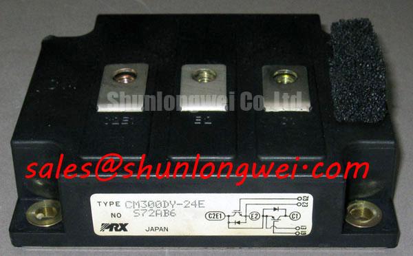
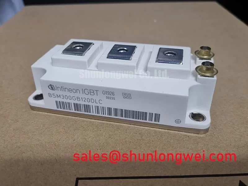
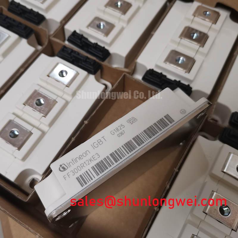
Start incoming inspection with the module disconnected from every power source: confirm the marking, inspect the case and terminals for mechanical damage, and record the cold-state resistance and diode-test readings against a known-good reference. The Infineon FF300R12KE3G is specified as a 1200.0 V, 300.0 A IGBT Module, with the package identified as Module in the supplied product data. These are official specification values; they do not, by themselves, define the allowable current at every switching frequency, duty cycle, case temperature, or cooling condition.
For a repair assessment, verify the original circuit position before applying a test voltage. The terminal polarity, gate connections, auxiliary terminals, and any integrated diode path must be checked against the applicable Infineon documentation for the exact device version. A multimeter diode range can help identify an unexpected open or short path under controlled, de-energized conditions, but it is not a substitute for a rated semiconductor curve tracer or an insulated high-voltage test procedure.
Transient thermal impedance is a time-dependent response rather than a single fixed resistance. During a short overload pulse, junction temperature rises according to the device thermal network, pulse duration, starting case temperature, and the cooling assembly. The required assessment should therefore use the manufacturer’s transient thermal impedance curves and the actual pulse profile. A multi-RC thermal model may be used as an Engineering Calculation to estimate peak junction temperature, but the result remains dependent on the validated thermal parameters and measured mounting conditions.
In forklift traction or electric material-handling equipment, regenerative braking can return energy to the DC link, while a braking chopper and resistor may absorb excess energy when the battery or DC bus cannot accept it. Designers should verify the braking resistor duty cycle, chopper switching pattern, DC-link voltage, and cooling airflow as a complete system. The module’s official voltage and current ratings should not be interpreted as a guaranteed braking-resistor power rating.
Minimize parasitic inductance in the commutation path and keep high-current conductors physically controlled to reduce turn-off overshoot. The required creepage distance, clearance, insulation system, and enclosure spacing are system-dependent and must be checked against the working voltage, pollution environment, altitude, and applicable safety standard. For design reference, consult the linked IGBT Design & Integration material together with the relevant manufacturer documentation.
Bench Tip: Use ESD protection, discharge the DC link fully, and compare cold-state measurements with a documented good module before connecting a gate driver or applying bus voltage.
FF300R12KE3G Circuit Protection and Reliability: Calibrating SCSOA Overcurrent Protection
Short-circuit protection must be calibrated around the complete gate-drive loop, current sensor, desaturation or overcurrent detection method, driver delay, and the module’s documented short-circuit safe operating limits. The supplied product information confirms the 1200.0 V voltage class and 300.0 A current rating, but it does not provide a verified short-circuit withstand time. A specific protection interval, including a sub-10-microsecond claim, should therefore be taken only from the applicable Infineon datasheet or application note for this exact part.
Type I and Type II protection strategies can be evaluated where the drive system requires staged fault handling. A controlled soft turn-off may reduce the rate of current change and limit inductive voltage stress, while a faster protection path may be required for severe faults. The gate resistor, driver current, detection blanking, fault latch, and turn-off profile must be selected from measured waveforms rather than copied as universal values.
During commissioning, capture collector-emitter voltage, gate-emitter voltage, phase current, and fault timing with suitably rated probes. Check whether the measured peak voltage remains within the manufacturer’s dynamic operating boundaries under the actual DC-link condition. If the waveform changes materially with cable length, temperature, or load current, investigate commutation inductance, sensor placement, driver reference integrity, and gate-loop coupling before altering protection thresholds.
Switching frequency and ambient temperature directly affect the thermal budget. The requested frequency range of 2 kHz to 16 kHz should be treated as an evaluation range, not as a confirmed operating guarantee for this module. Engineers should calculate switching and conduction losses from the official electrical characteristics, then verify the heatsink, interface material, fan performance, and enclosure airflow through temperature measurements. Any derating curve must be based on the manufacturer’s published data and the measured thermal interface.
The Infineon IGBT Modules & Discretes Official Portfolio provides manufacturer-level product context. A same-family reference such as FP10R12KE3 may be reviewed for comparison, but electrical interchangeability must be established from pin configuration, ratings, thermal data, gate requirements, mechanical fit, and the original inverter design.
Field Diagnostics and Commissioning: Suppression of DC-Link Spikes in FF300R12KE3G Topologies
When a repaired traction inverter produces an unexpected overvoltage alarm, first measure the DC-link voltage at the module terminals and compare it with the controller’s recorded value. Probe placement matters: a long probe ground lead can introduce ringing that does not represent the actual semiconductor terminal waveform. Use a properly rated differential probe and examine the switching node during acceleration, regenerative braking, and controlled no-load operation.
Long motor leads can create distributed impedance effects and reflections. These effects may increase terminal ringing, particularly when cable construction, motor impedance, output filter configuration, and switching edge rate are not well matched. A claim that a terminal spike will reach a particular multiple of VDC is not a universal property of this part and requires measurement on the installed system.
Output chokes, dv/dt filters, and motor-side filters should be sized from the drive voltage, motor insulation requirements, cable length, switching behavior, common-mode current, and thermal duty of the filter components. This is an Engineering Recommendation to evaluate the entire motor-cable topology rather than placing an unverified filter value directly at the module. Confirm that the filter does not create excessive circulating current, resonance, or additional switching loss.
For field troubleshooting, inspect the DC-link capacitor connections, laminated bus structure, gate-driver return path, snubber condition, and phase-leg symmetry. Compare all phases under the same operating point. An abnormal difference may indicate layout imbalance, a sensing problem, a damaged passive component, or a gate-drive timing issue; it should be verified against a known-good signal path before the IGBT module is condemned.
Keep the high-voltage power loop physically separated from control wiring and maintain the clearance and creepage required by the system insulation design. The correct spacing is determined by working voltage, pollution degree, material group, altitude, and enclosure construction. The Infineon IGBT Modules Overview can be used as a manufacturer reference point, while the final insulation assessment belongs to the equipment designer.
Benchtop Waveform Tuning: Reinforced Insulation Barrier Integrity on FF300R12KE3G Drives
Before waveform tuning, isolate the control supply from the power stage and verify that the oscilloscope, differential probes, driver board, and test fixture are rated for the intended common-mode voltage. The supplied specifications identify this product as a high-power IGBT Module rated at 1200.0 V and 300.0 A; they do not confirm a reinforced isolation rating, a 5 kV withstand value, or a CMTI value above 100 kV per microsecond.
Isolation performance belongs to the complete gate-drive assembly. The isolator, creepage path, PCB geometry, power supply insulation, connector arrangement, and mechanical contamination all influence the result. Designers should verify the required isolation class and test voltage from the driver and equipment documentation, then validate the assembled barrier using an approved production or laboratory procedure. Do not attribute the isolation capability of a digital isolator to the IGBT module itself.
During bench tuning, observe the gate-emitter waveform at the module terminals, not only at the driver output. Check for unexpected gate movement during the opposite switch transition, regenerative braking, and rapid load changes. If a false trigger appears, investigate common-mode coupling, inadequate driver reference connections, probe capacitance, control-board grounding, and excessive power-loop voltage movement. The appropriate mitigation may involve layout changes, gate-loop damping, isolated supply improvements, or a revised switching profile; the final choice must be validated with the actual hardware.
Reinforced insulation, EMC behavior, and CMTI compliance are equipment-level subjects. A discrete module cannot independently claim compliance with a complete CISPR or EN 55011 installation. Record the tested bus voltage, load state, switching condition, probe arrangement, and environmental state so that future repair comparisons use the same measurement boundary.
Safety Interlock Note: Do not connect or remove gate-drive wiring until the DC link has been isolated, discharged, and verified with an appropriately rated meter.