

Content last revised on October 23, 2026
FF800R12KE3 Circuit Protection & Reliability: Calibrating Negative Gate Bias vs Active Miller Clamping
When a traction inverter trips during turn-off, first isolate the power and gate-drive supplies, discharge the DC link, and verify the absence of hazardous voltage before comparing the gate-emitter impedance of the suspect phase with a known-good phase and reconnecting the control board. The FF800R12KE3 is an Infineon IGBT module rated at 1200 V VCES, with a specified 10 µs short-circuit withstand time under the datasheet test conditions; these figures define important device boundaries, but the complete protection response is determined by the gate driver, current sensor, desaturation circuit, and layout.
High dv/dt at the switching node can couple through the Miller capacitance and raise the inactive IGBT gate voltage. If the complementary device is still conducting, this unwanted gate movement can contribute to cross-conduction. A negative gate bias is one possible Design Consideration for increasing off-state immunity, while an active Miller clamp provides a low-impedance path that holds the gate close to its intended off-state potential during the critical switching interval. The negative bias value must be selected from the driver and module documentation; it should not be treated as a universal setting for every inverter.
During field troubleshooting, inspect the gate waveform directly at the module terminals rather than at the driver output alone. A difference between those two points may indicate gate-loop inductance, connector resistance, poor reference routing, or an unintended return-current path. Keep the power commutation loop and gate-drive loop physically separated, use a short Kelvin-style gate return only where the applicable module and driver arrangement support it, and avoid routing the high-voltage switching node parallel to sensitive gate traces.
Optocouplers and digital isolators also require attention. Their common-mode transient immunity must be evaluated against the actual switching environment, including isolation capacitance, gate-loop placement, supply decoupling, and the propagation delay of the fault path. A driver that appears functional at low voltage can behave differently when the collector-emitter voltage changes rapidly. When reviewing an isolated control board, compare the turn-on and turn-off timing of both channels, check the fault latch response, and verify that the active Miller clamp does not interfere with the intended gate discharge path.
The official Infineon IGBT portfolio provides the appropriate manufacturer context for module technology and application documentation. For a replacement assessment, compare not only the voltage and current ratings but also gate-drive requirements, terminal arrangement, thermal interface, and short-circuit behavior. The FF500R12KE4 may be reviewed as a separate same-voltage-class reference, but it should not be treated as a drop-in substitute without a mechanical and electrical compatibility check.
FF800R12KE3 Thermal-Electrical Optimization: Thermal Paste Degradation Prevention and Practical Tuning
Thermal problems in a high-current module often begin at the interface between the baseplate and heatsink, so remove the module and inspect the contact pattern instead of assuming that a high current rating guarantees sufficient cooling. The FF800R12KE3 has an official typical saturation voltage of 1.70 V VCE(sat) under the specified datasheet conditions and an official IGBT junction-to-case thermal resistance of 0.031 K/W. These values support thermal evaluation, but junction temperature still depends on switching loss, conduction duty, coolant or airflow conditions, heatsink flatness, and the complete mounting system.
A Design Consideration for thermal interface material is to apply a controlled, continuous film rather than a thick layer intended to compensate for a distorted baseplate. An approximate film thickness of 50 to 100 µm may be used as an engineering starting reference only when consistent with the module mounting instructions, selected material, and heatsink surface condition. Excess material can increase thermal resistance and migrate toward the mounting area, while insufficient material can leave voids that create localized hot spots.
Clean both mating surfaces with a compatible process, inspect for scratches or raised areas, and place the module on the heatsink without using the screws to pull a visibly misaligned assembly into position. Tighten the mounting screws progressively in a diagonal sequence so that the baseplate seats evenly. The final torque must follow the module mechanical documentation, screw grade, washer arrangement, and heatsink thread condition.
Field Alert: Do not use the mounting screws to correct baseplate misalignment, and never insert or remove the gate connector while the DC link or isolated driver supply remains energized.
Electrical and thermal tuning must be handled together. A higher gate resistance can reduce ringing and switching stress but may increase switching loss; a lower resistance can shorten transition time while increasing overshoot and electromagnetic disturbance. Select the initial gate network from the driver capability and the module gate-charge data, then evaluate the actual gate-emitter and collector-emitter waveforms under controlled switching tests.
For a high-side driver using bootstrap power, size the capacitor from the gate charge required for the commanded switching pattern, driver quiescent current, leakage, refresh interval, diode behavior, and allowable supply droop. The capacitor must retain adequate driver supply during the complete high-side conduction interval, not only during the first gate pulse. The bootstrap diode reverse-recovery behavior can inject a disturbance into the driver supply, so observe the supply waveform at the driver pins and verify that its recovery current does not couple into the gate loop.
In a traction inverter evaluation, the module may be considered for high-power switching positions subject to the original equipment design, cooling system, insulation coordination, and control protection. The Infineon EconoDUAL™ 3 reference page can help engineers compare package-family information, while the exact FF800R12KE3 installation must follow its applicable mechanical and electrical documentation.
Transient Dynamics & Electrical Design: Short-Circuit Energy Let-Through Matching on FF800R12KE3
Coordinate the semiconductor fuse, gate-driver protection, and DC-link architecture before placing a replacement module into service. The official 10 µs TSC rating for the FF800R12KE3 is a short-circuit withstand specification under the datasheet test conditions, not a promise that any external fuse will clear within that interval. Fuse total clearing I²t, driver detection delay, contactor behavior, cable inductance, DC-link capacitance, and the fault current rise rate all influence the energy imposed on the module.
The correct engineering task is to compare the protection chain as a time sequence. The gate driver must detect the fault, initiate a controlled turn-off, and prevent a second gate command while the fault latch remains active. The semiconductor fuse must be selected using its manufacturer-clearing characteristics at the applicable DC voltage and prospective fault current. A fuse with an acceptable nominal current can still be unsuitable if its clearing energy or interruption behavior does not coordinate with the module and DC-link arrangement.
During commissioning, use an isolated differential voltage probe and a current measurement method suitable for the expected transient. Check the collector-emitter overshoot, gate voltage during desaturation, driver supply collapse, and the timing between fault detection and gate removal. If a protection event produces inconsistent results between phases, inspect current-sensor placement, auxiliary supply impedance, optical or digital isolation delay, and the fault-reset logic rather than assigning the event to the IGBT alone.
Minimize stray inductance in the commutation path to reduce turn-off overshoot, and provide physical clearance around high-voltage conductors according to the system insulation and pollution environment. The peak switching voltage must be verified against the module voltage rating at the applicable DC-link condition during testing. High-altitude operation, cosmic-ray effects, single-event burnout, FIT values, and long-term lifetime require application-specific qualification data; they should not be represented by unsupported numerical claims for this module.
For engineers comparing silicon and wide-bandgap switching approaches, the Wide Bandgap Revolution reference provides broader context on switching speed, parasitic effects, and design tradeoffs. It does not replace the FF800R12KE3 electrical and protection requirements.
Transient Dynamics & Electrical Design: Main Terminal Pinout Mechanical Alignment on FF800R12KE3
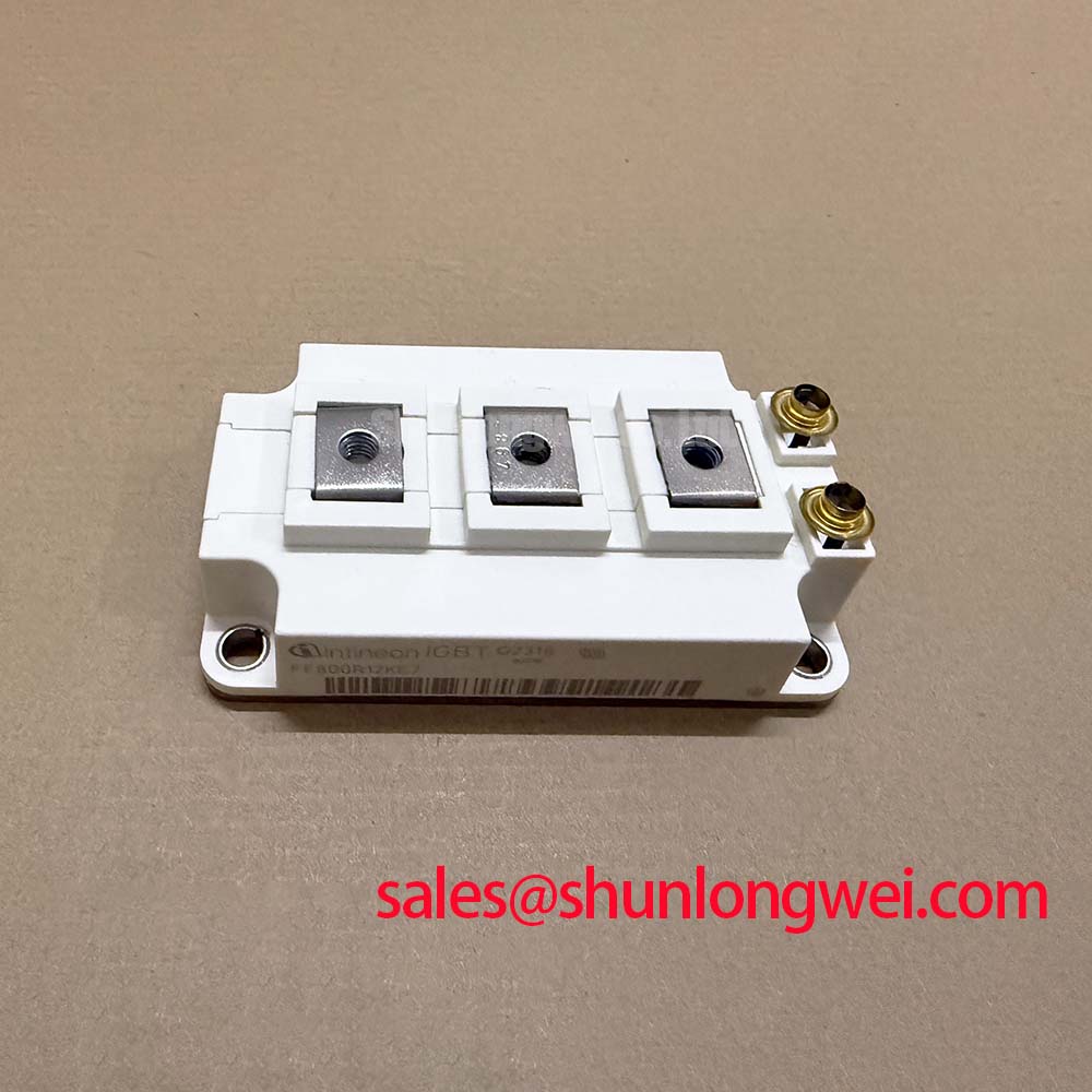
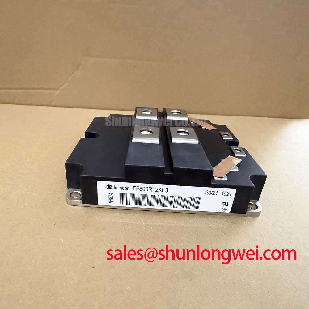
Align the main terminals, busbars, and gate connections before tightening any fastener; forcing a busbar into position can transfer mechanical stress into internal joints and create an intermittent fault that is difficult to reproduce. Confirm the original equipment terminal identification from the module marking and wiring documentation, then verify that collector, emitter, and gate connections match the inverter topology before applying control power.
The power busbar should sit naturally over the module terminal without side loading. Check thread engagement, washer seating, busbar parallelism, and clearance from adjacent conductors. The fastening arrangement must provide stable electrical contact through vibration and thermal cycling without exceeding the manufacturer’s mechanical limits. Do not substitute a different screw, washer, or busbar thickness without reviewing the resulting clamping condition and insulation clearance.
After mechanical installation, inspect the gate-emitter control pair separately from the power terminals. A long or poorly supported gate lead can increase ringing even when the power busbar is correctly installed. Keep the gate return path adjacent to the gate path where the module interface permits, and prevent the control wiring from sharing an uncontrolled return route with high-current commutation current.
Before energizing the DC link, check continuity from the driver output to the module gate terminal, confirm the intended emitter reference, and verify that no connector pin has been displaced during installation. With the power stage disabled, compare the phase-leg control signals and fault interlock behavior. Then introduce voltage under a controlled test plan while monitoring gate voltage, switching-node behavior, and thermal response.
The 800 A continuous collector-current rating at Tc = 80°C is an official specification, while the permissible operating current in a particular traction inverter remains dependent on cooling, switching frequency, duty cycle, overload profile, and enclosure conditions. Engineers evaluating this module for high-speed rail or heavy freight locomotive traction inverters should match the complete mechanical envelope and protection architecture, not only the headline current rating.