
Content last revised on October 28, 2026
Assessing Atmospheric Neutron Radiation Risk in 6MBI550V-120-50 Applications
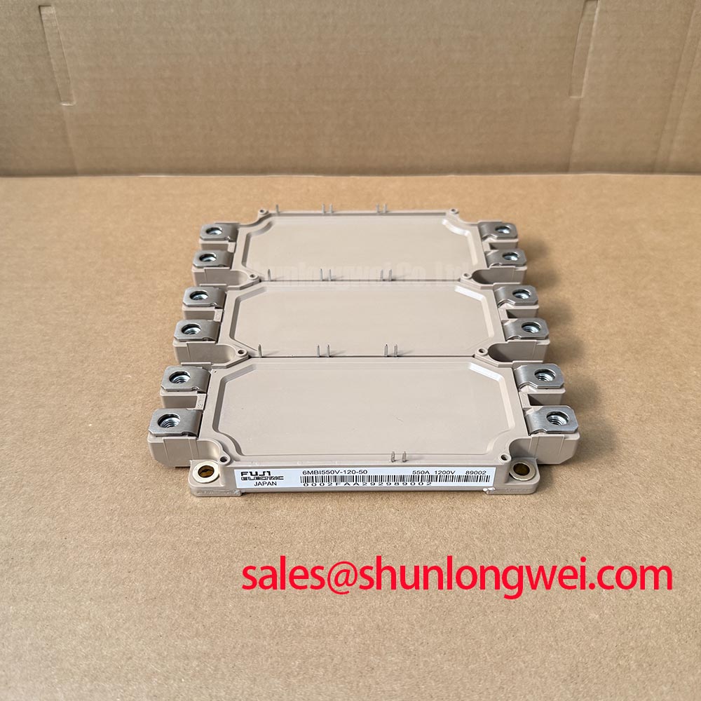
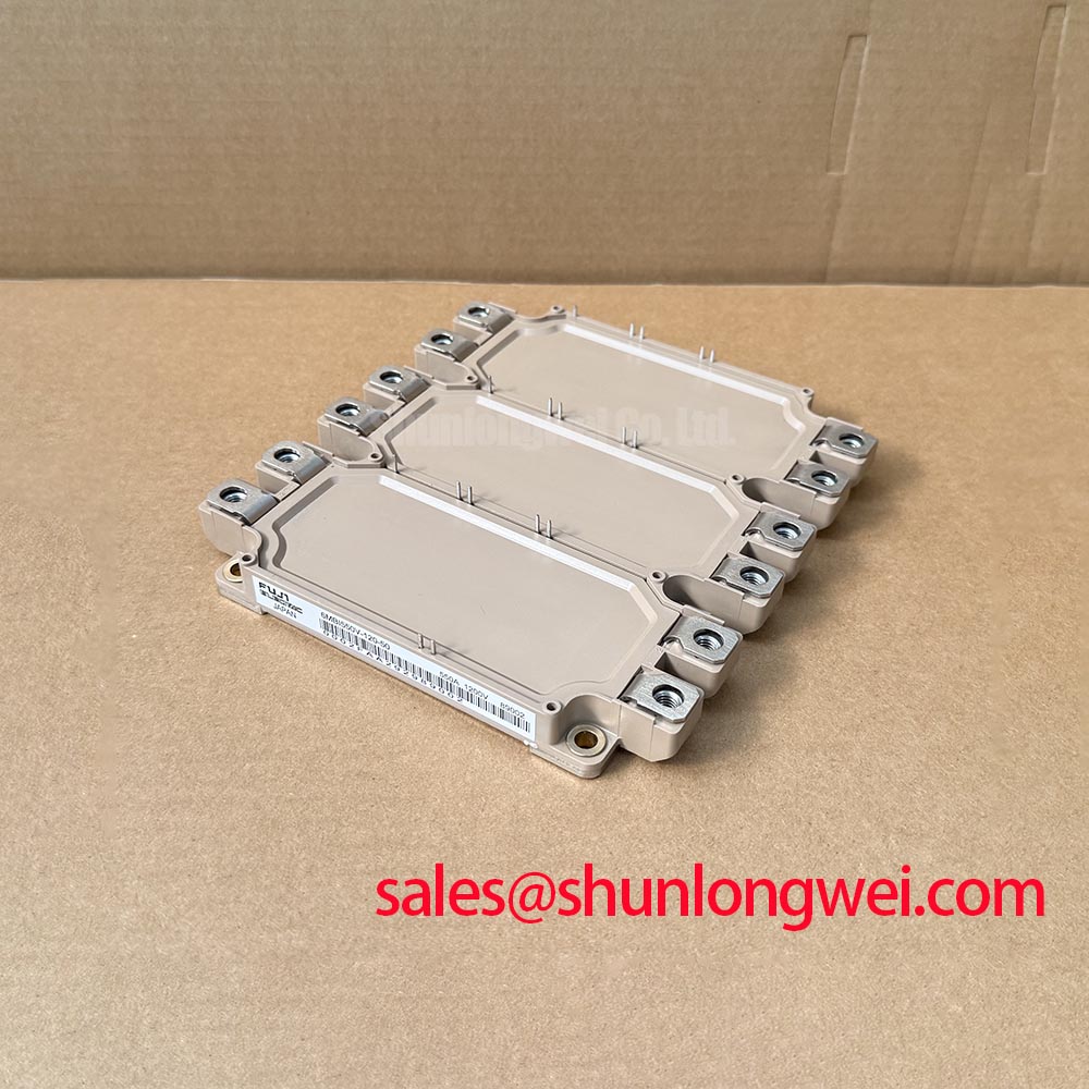
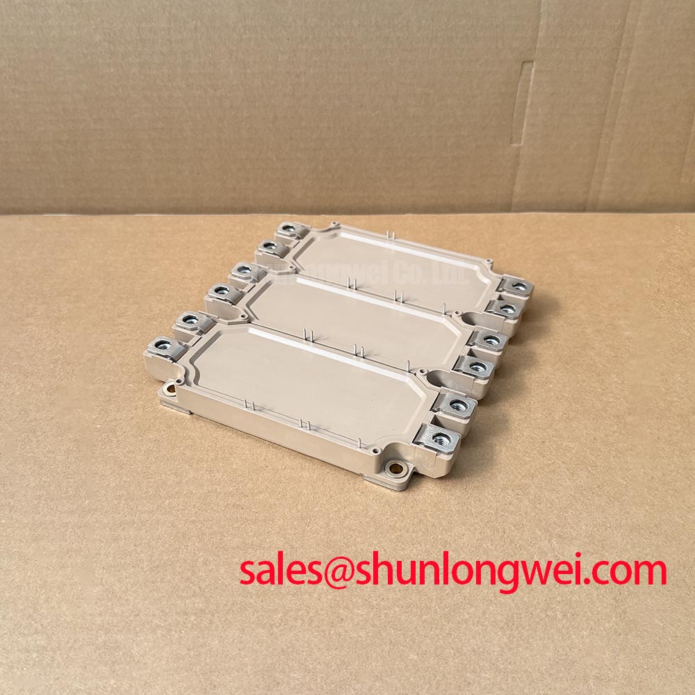
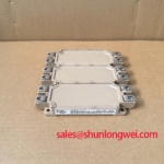
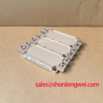
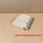
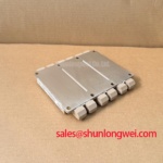
With the DC link isolated and verified discharged, compare the module marking with the equipment bill of materials before disconnecting the gate harness or loosening the power terminals. The Fuji Electric 6MBI550V-120-50 is an IGBT module with a 1200 V voltage rating and a 550 A collector current rating under the specified datasheet conditions. The electrical rating conditions, terminal drawing, mechanical dimensions, and installation limits belong to the model-specific datasheet.
For replacement assessment, preserve the complete 6MBI550V-120-50 designation rather than matching only the voltage and current. Record the existing busbar arrangement, gate connections, cooling interface, and protection settings before removal. These observations establish the equipment configuration against which the replacement must be evaluated, without treating a package description as proof of mechanical or electrical interchangeability.
Separate a recorded protection trip from confirmed semiconductor damage before attributing an unexplained shutdown to an environmental mechanism. As a Design Consideration, preserve the fault timestamp, DC-link history, switching state, cooling condition, and gate-driver diagnostics. Correlating those records can reveal overvoltage, interrupted cooling, or unintended switching that would otherwise be obscured by a broad description such as “random module failure.”
For installations at elevated altitude, atmospheric-neutron-related single-event burnout belongs in a manufacturer-supported reliability assessment, not a calculated percentage taken from the voltage rating. A meaningful failure-in-time assessment requires applicable device susceptibility data, the environmental neutron spectrum, and the actual blocking-voltage exposure. An altitude threshold alone does not establish a safe operating boundary or a module-specific failure rate.
DC-link headroom should therefore be assessed against both the recurring blocking voltage and measured switching excursions. Reducing electrical stress is a Design Consideration, but no universal derating percentage follows from the 1200 V rating. Keep the environmental reliability assessment distinct from clearance and creepage selection: atmospheric radiation and electrical insulation coordination are different engineering problems.
When evaluating this module for a multi-megawatt offshore or onshore wind-turbine full-scale converter, designers should check the converter architecture, voltage sharing where applicable, cooling capacity, and equipment qualification requirements. The IGBT Design & Integration reference provides broader context for gate-drive, thermal, and topology reviews; equipment acceptance still depends on the particular converter and its validated operating envelope.
Unpowered Bench Screening: Multimeter Diode Checks on 6MBI550V-120-50
Disconnect external paths that could influence a diode-mode reading, then identify each measurement pair from the terminal drawing. As a Design Consideration, compare the corresponding switching positions using the same meter, polarity, and connection conditions. Where the circuit diagram identifies an antiparallel diode, a directional response can support preliminary screening, but the displayed value is not a datasheet forward-voltage test.
Look for repeatable differences between equivalent paths rather than applying an invented pass threshold. An unexpectedly low reading can result from a parallel circuit, residual gate charge, or a damaged semiconductor; an open indication can also reflect the meter’s test capability or an incorrect terminal pair. Resolve the connection conditions before interpreting the result. A handheld meter cannot establish high-voltage blocking integrity or switching performance.
Gate-to-emitter screening should similarly remain qualitative unless performed with the specified leakage-test conditions. Disconnect the driver, apply appropriate electrostatic handling precautions, and compare the measurement with the intended gate circuit. Do not mistake the absence of a visible meter response for proof that the gate insulation meets its rated limits.
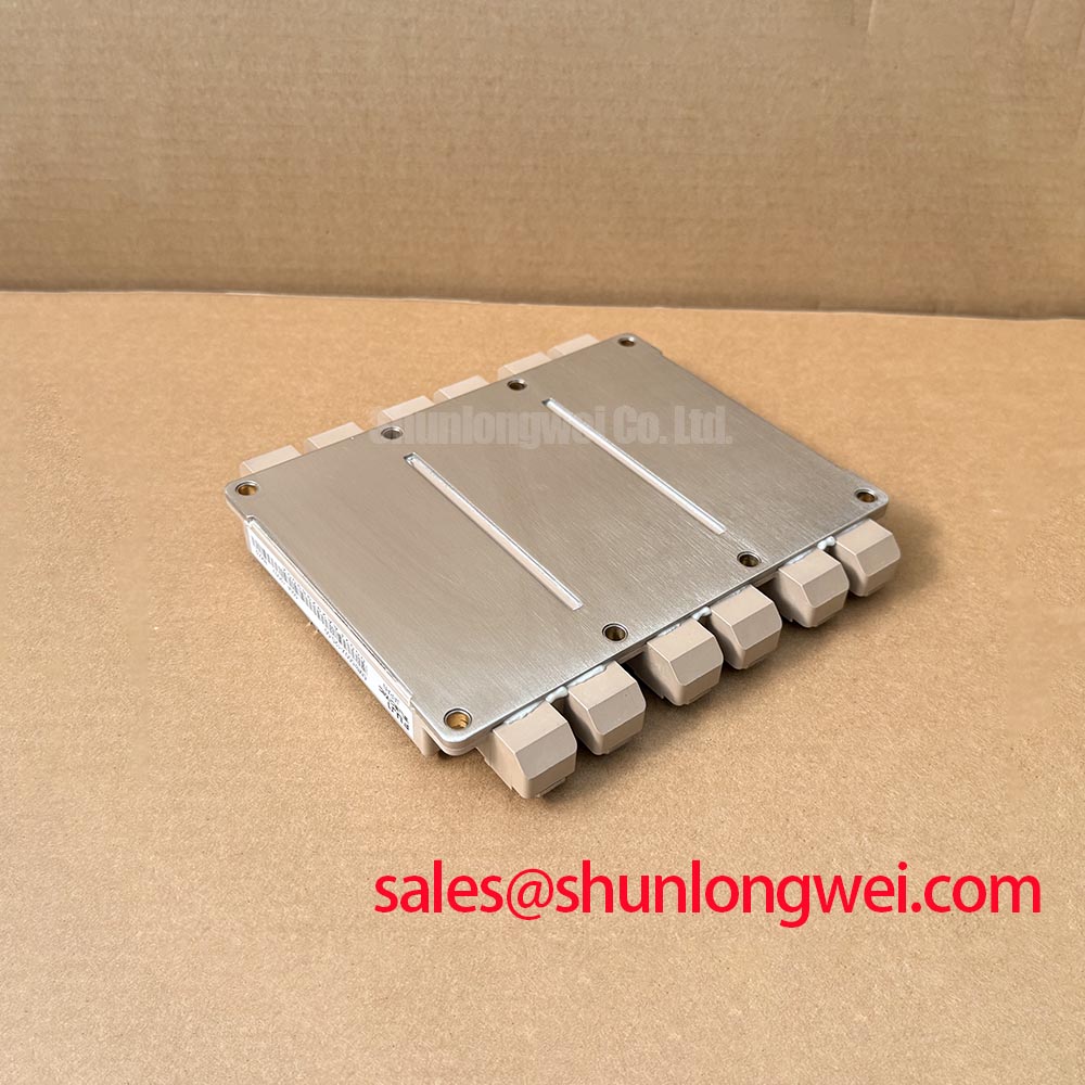
Before mounting, inspect the mating surfaces for contamination, burrs, and uneven contact. Thermal interface material thickness should follow the approved material and mounting instructions; a generic film thickness is not an Official Specification for this module. Tighten progressively in the documented sequence, using the specified hardware and torque rather than transferring values from another enclosure.
In a replacement comparison, 6MBI75S-120-01 is a separate Fuji model to evaluate, not a verified direct replacement for 6MBI550V-120-50. Compatibility requires matching the electrical duty, circuit configuration, terminal positions, mechanical drawing, gate-drive requirements, and thermal path. Similar naming or a shared voltage class does not establish interchangeability.
Field Diagnostics & Commissioning: Gate Drive Loop Geometry for 6MBI550V-120-50
Trace the driver output and its return together on the actual assembly, paying particular attention to any segment shared with the load-current path. As a Design Consideration, shared emitter inductance can introduce a voltage into the effective gate-emitter loop during current transitions. That coupling can distort the commanded gate voltage and complicate interpretation of apparent driver faults.
Use a dedicated auxiliary emitter connection only where the module terminal drawing identifies one. Do not infer a Kelvin connection from the package family or copy the wiring of another module. Where the documented interface supports a separate driver return, route it with the gate conductor and keep the loop away from high-current commutation paths. Final routing must also satisfy the equipment’s insulation requirements.
Observe gate-emitter voltage at the relevant module terminals with an appropriate differential measurement arrangement. Probe connections and common-mode limitations matter: apparent ringing can be introduced or exaggerated by the measurement setup. Compare the commanded switching edge with the gate waveform and power-terminal response before changing the driver circuit.
Miller-induced gate movement should be evaluated during the opposing device’s voltage transition. The driver’s turn-off impedance, local return path, and available suppression functions should be considered together. Any adjustment must remain within the module’s gate limits and the driver’s capabilities, with acceptance based on measured switching behavior rather than a generic resistor prescription.
Pro Tip: Keep commutation paths compact and geometrically balanced where the topology permits, then verify turn-off voltage headroom with a controlled double-pulse test.
If the existing driver uses a bootstrap supply, check its recharge opportunity and supply behavior across the operating duty cycle. That is a driver-system assessment, not a module feature. Protection timing and gate-supply stability should be demonstrated before increasing switching stress during commissioning.
6MBI550V-120-50 Circuit Protection & Reliability: Evaluating Diode Recovery and Commutation Stress
Capture diode commutation current and the associated switching-node voltage under controlled conditions before selecting a snubber or changing turn-on gate resistance. As a Design Consideration, reverse-recovery behavior depends on the preceding forward current, junction temperature, and imposed commutation rate. A recovery waveform measured at one operating point should not be treated as a fixed characteristic across the equipment’s entire load range.
Examine peak reverse-recovery current, the subsequent current decay, and voltage ringing together. An abrupt recovery transition can interact with stray inductance, but a ringing trace alone does not identify the diode as the sole cause. Busbar geometry, probe placement, gate-drive behavior, and nearby capacitance also influence the observed waveform.
Adjusting turn-on gate resistance can change commutation stress while also changing switching loss. An RC snubber introduces its own pulse-energy, dissipation, and voltage-rating requirements. Evaluate either measure against the measured operating envelope and cooling capability; there is no model-independent resistance or capacitance value that establishes compatibility.
Fuji Electric’s RC-IGBT Modules information addresses a distinct device technology, while its Brake Chopper IGBT Modules page concerns another circuit role. Neither establishes the internal diode construction, recovery values, or braking capability of this particular model.
For protection review, distinguish repetitive commutation from abnormal surge events. Do not convert the 550 A current rating into an assumed surge-current withstand limit or a guaranteed restart interval after a trip. Establish fault-clearing behavior and restart permission from the applicable device limits, thermal assessment, and equipment protection logic. Retain the measured waveforms and test conditions with the replacement record so subsequent maintenance decisions use the same electrical baseline.