
Content last revised on October 27, 2026
Field Diagnostics and Commissioning: Mitigating Commutation Turn Off Voltage Spikes in 6MBP50VCA120-51 Topologies
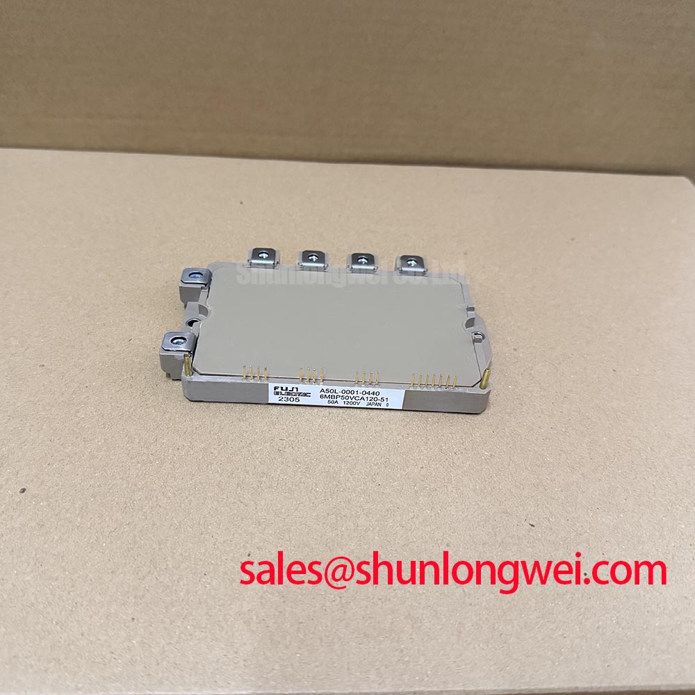
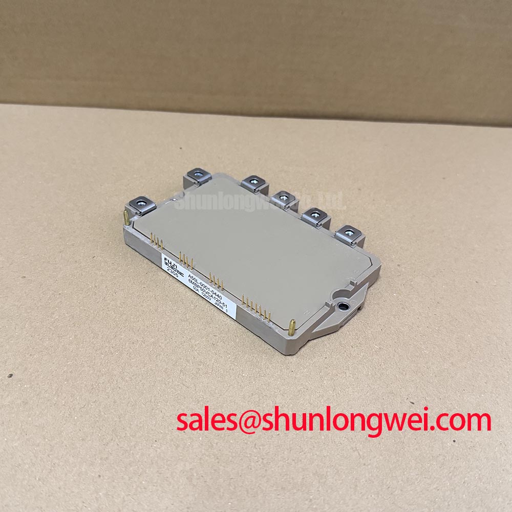
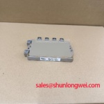
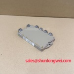
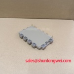
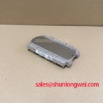
When a heavy duty variable frequency AC motor drive reports an overvoltage trip during deceleration, first check whether regenerative energy is raising the DC link voltage and whether the drive’s braking or regeneration system is operating correctly. If irregular current or voltage spikes occur at commutation, investigate the switching node and control supply return paths rather than replacing the power module immediately. Confirm the installed part marking, isolate and safely discharge the DC link, and compare the cold state terminal behavior with a known good phase position. The device identified for this application is the Fuji Electric 6MBP50VCA120-51, a 1200 V, 50 A intelligent power module (IPM) with integrated gate drive and protection functions. These ratings do not replace the operating conditions and limits established by the module documentation and complete drive.
Commutation stress is often exposed when the antiparallel diode current changes rapidly. Reverse recovery current, represented in switching analysis by Irrm, can combine with commutation loop inductance and produce a voltage excursion across the switching devices. A snappy recovery event can create a high rate of current change, increasing conducted and radiated noise while reducing the available voltage margin. The correct field task is to capture the switching voltage at the accessible module power terminals with a suitable differential probe and compare it with the control input timing and phase current during the same event.
Use the measured waveform to separate a device related behavior from an installation related behavior. A peak that changes substantially when the probe connection arrangement, control supply return routing, or motor load changes may point toward measurement or layout interaction. A repeatable overshoot synchronized with turn off should direct attention to the commutation loop, DC link capacitor placement, laminated busbar geometry, and the diode recovery path. Any RC snubber should be selected from measured ringing frequency, energy, thermal loading, and system insulation requirements. It should not be treated as a universal accessory for every installation of this module.
In modules with accessible gate connections, tailoring turn on gate resistance can reduce the rate at which recovery current is forced through the opposing path, but it also changes switching loss and thermal behavior. The 6MBP50VCA120-51 uses integrated gate drivers, so this is not an external adjustment to assume is available. Follow Fuji Electric’s IPM interface requirements and evaluate control supply integrity, input timing, and the external commutation loop during controlled switching tests.
The Fuji Electric discussion of PIM power integrated module structures provides context for a different module category; it is not the interface documentation for this IPM. The complete drive remains responsible for its own EMC behavior, insulation coordination, and switching validation. The module itself should not be described as independently certified for a complete CISPR or EN 55011 installation.
Assembly Integrity and Layout Architecture: Preventing High di/dt Control Interface Transients
The 6MBP50VCA120-51 integrates its gate drivers, so external control connections must not be treated as discrete IGBT gate and Kelvin emitter terminals. Follow the manufacturer’s terminal identification for each control supply, reference, input, and fault connection. Do not infer a Kelvin function or an accessible internal gate connection from terminal position alone.
This distinction matters during fast current transitions. Voltage developed across shared return inductance can disturb the control supply reference and create ground bounce. Symptoms can include incorrect input recognition, fault indications, or a control signal that looks clean at the controller but becomes distorted at the module interface. Measure control inputs and supply voltages relative to their designated module reference terminals, using instrumentation suitable for the potential and common mode transients involved.
Keep the external control supply and signal loops compact, with each outgoing path and its return arranged as a closely coupled pair where appropriate. Separate power commutation conductors from sensitive control wiring and avoid sharing control return paths with load current. The objective is to minimize parasitic loop inductance so that the interface sees a stable reference during high di/dt transitions. Final spacing, insulation distance, and conductor geometry are system decisions governed by working voltage, pollution environment, enclosure construction, and the applicable safety design.
Parallel module operation requires additional care and should only be considered where the manufacturer’s application guidance supports it. A positive temperature coefficient of conduction voltage in an IGBT can support static current sharing under suitable operating conditions, but matching devices alone does not correct unequal busbar resistance, differences in switching timing, or differences in thermal coupling. Integrated drivers and protection functions also require coordination. Where parallel operation is supported, use symmetrical DC link and output paths, equivalent control routing, and a mechanically consistent heatsink interface. Compare the individual module currents during a controlled load test rather than assuming that identical part numbers guarantee equal dynamic current sharing.
The selection review may also include the related 6MBP50TEA120 when the equipment documentation identifies a compatible Fuji Electric module family. This is a neutral comparison path, not a substitute recommendation. Pin assignment, electrical ratings, mechanical envelope, control interface requirements, and protection behavior must be checked against the original drive design before any interchange decision.
For background on driver reference routing, Miller effect control, and commutation loop placement, engineers can consult Precision Gate Drive Design. Guidance about external gate components must not be applied directly to this IPM’s control inputs; the relevant implementation remains dependent on its documented interface, control board, busbar, and module assembly.
💡 Pro Tip: Capture the control input and control supply waveforms at the module interface while the power stage is switching; a controller board waveform alone can hide return path induced transients.
6MBP50VCA120-51 Operational Boundaries: Evaluating Thermal Stress Monitoring across High Current Limits
Terminal heating should be investigated as an assembly condition before it is attributed to the semiconductor die. A bolted joint with contamination, uneven clamping, damaged plating, or conductor misalignment can generate localized heat even when the phase current is below the module’s 50 A rated collector current. The rating itself is not a complete operating limit because conduction loss, switching loss, case temperature, cooling arrangement, duty cycle, and transient loading all affect junction temperature.
A micro ohmmeter can be used to compare the resistance of each bolted power connection under a controlled, de energized condition. Acceptance limits should come from the applicable joint design or maintenance procedure, not from the module’s semiconductor ratings. The useful result is the comparison between equivalent terminals and the change observed after mechanical correction. The test current, probe placement, surface condition, and joint temperature should be recorded so that readings remain comparable.
Thermographic inspection should be performed after the drive reaches a defined steady operating condition and should compare equivalent phase terminals, busbar interfaces, and heatsink regions. A bright localized area at one terminal may indicate contact resistance, conductor imbalance, or airflow obstruction, while a broader temperature rise may be associated with total loss or cooling performance. Infrared emissivity settings, reflective surfaces, enclosure airflow, and camera angle can influence the image, so temperature conclusions should be checked with an appropriate contact or calibrated reference measurement.
For pulsed operation, the transient thermal impedance path is more informative than a simple steady state temperature estimate. The engineer should evaluate the relevant Zth network over the actual pulse width, repetition pattern, case temperature, and cooling boundary. This allows the peak junction temperature margin to be assessed without treating the rated collector current as a guarantee for every waveform. A thermal model should be correlated with measured case or heatsink temperature during representative acceleration, deceleration, and load cycling.
If the module is considered for a bidirectional DC to DC battery charging or discharging stage, topology, control interface, and protection suitability must first be verified. In such an application, repeated thermal cycling can be influenced by current profile, switching frequency, cooling response, and the mechanical construction of the power assembly. Designers should monitor temperature rise across both power flow directions and should evaluate whether the thermal path returns to its starting condition between cycles. Specific lifetime hours or failure rates require an applicable reliability source and should not be inferred from the nominal voltage and current values.
During installation, use a clean, flat thermal interface and maintain even mechanical pressure across the module base according to the applicable Fuji Electric mechanical documentation. Do not compensate for a distorted heatsink by increasing fastener force. The resulting stress can affect the baseplate, terminal alignment, or semiconductor thermal path.
Field Diagnostics and Commissioning: High Frequency Common Mode Bearing Current in 6MBP50VCA120-51 Topologies
Long motor leads can transform a switching waveform into a transmission line problem. The cable impedance, motor input impedance, shield termination, and inverter output edge rate can interact to reflect energy along the cable. In unfavorable conditions, the motor terminal voltage may approach twice the applied inverter voltage step. That value is a possible system transient, not an operating rating of the 6MBP50VCA120-51, and it must be verified with a correctly rated differential measurement system.
Begin the investigation at both ends of the motor cable. Record phase to phase and phase to ground waveforms, then compare them with cable length, termination arrangement, switching state, and motor speed. A mismatch between the inverter output and the motor cable may produce ringing that is absent when the motor is replaced with a short laboratory connection. Common mode current can also travel through cable shields, motor frames, bearings, and protective earth paths, creating bearing current symptoms or interference in nearby control circuits.
Output chokes, dv/dt filters, or sine wave filters can change the cable interaction, but the suitable choice depends on the motor insulation system, carrier frequency, allowable voltage rise, filter losses, control response, and drive protection functions. Treat these components as system-level Design Considerations. Validate the filter with the actual cable and motor combination, including thermal performance and the effect on current regulation. A filter should not be described as an inherent feature of the Fuji power module.
Common mode bearing current should be assessed by examining the return path rather than only the phase voltage. Check shaft grounding arrangements, motor frame bonding, cable shield termination, and the continuity of the protective conductor. If a common mode choke is evaluated, its impedance over the relevant switching spectrum and its saturation behavior under the expected common mode and imbalance conditions should be established by the system designer. The module can be part of the switching source, but the resulting EMC and bearing current performance belongs to the complete drive and motor installation.
The 1200 V rating establishes the device voltage class, while the measured switching peak helps determine whether the installed topology is operating within its practical voltage margin. Use a controlled commissioning sequence with current limitation, temperature observation, and progressively representative motor loading. When an overvoltage trip persists, compare the DC link waveform, module terminal waveform, and motor terminal waveform to distinguish regenerative bus voltage rise from switching or cable transients. This evidence supports targeted changes to braking or regeneration arrangements, layout, control supply integrity, cable treatment, or output filtering without assigning a single cause prematurely.
The 6MBP50VCA120-51 is therefore evaluated as a Fuji Electric IPM module with a 1200 V voltage rating and a 50 A rated collector current under the manufacturer’s specified conditions. Integration decisions should be based on the original drive topology, verified terminal identification, measured switching behavior, thermal testing, and the mechanical requirements of the intended heavy duty variable frequency AC motor drive.