
Content last revised on September 12, 2026
Preventing Spurious Faults: Thermal Cycling Margins of Internal Braking Guidelines for 7D75D-050EHR
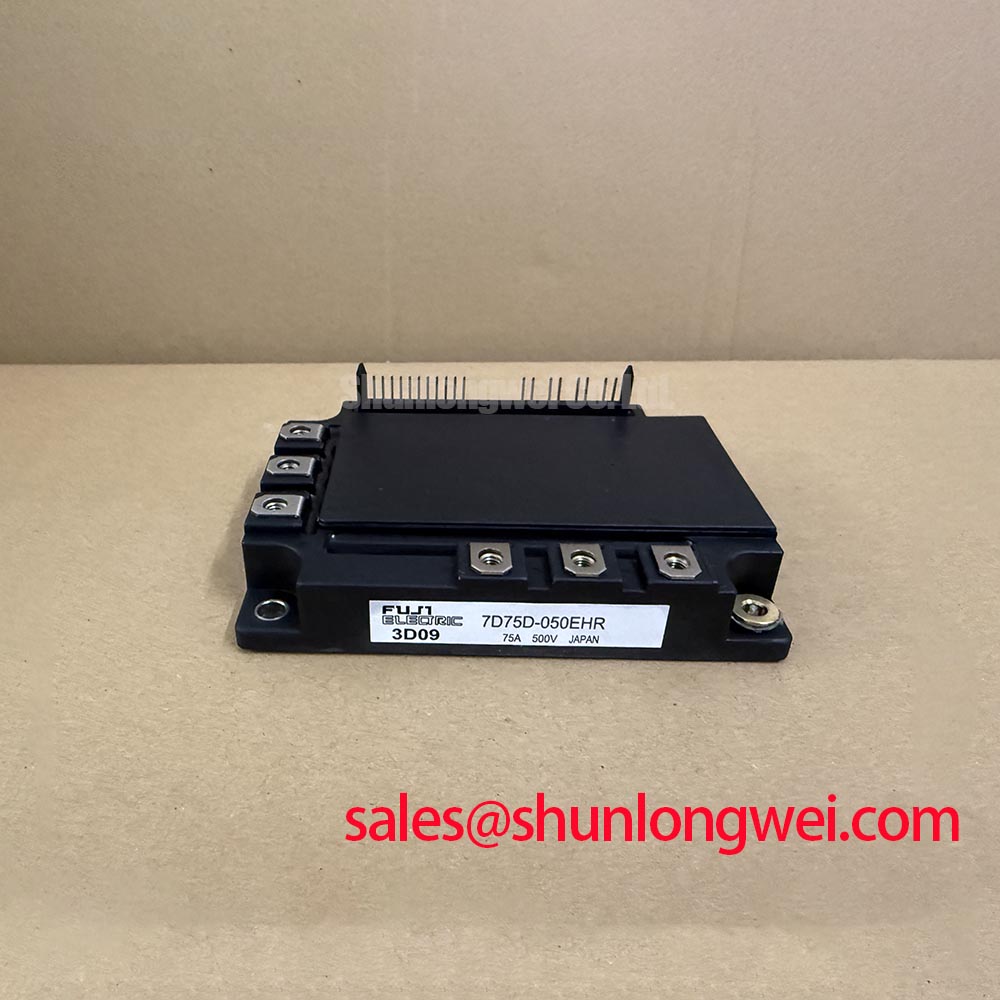
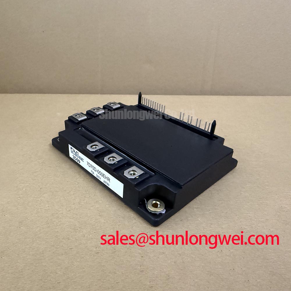
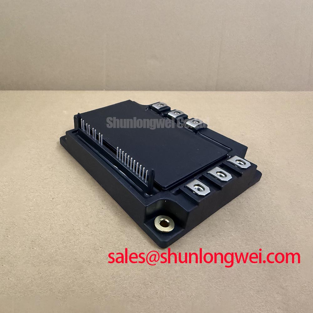
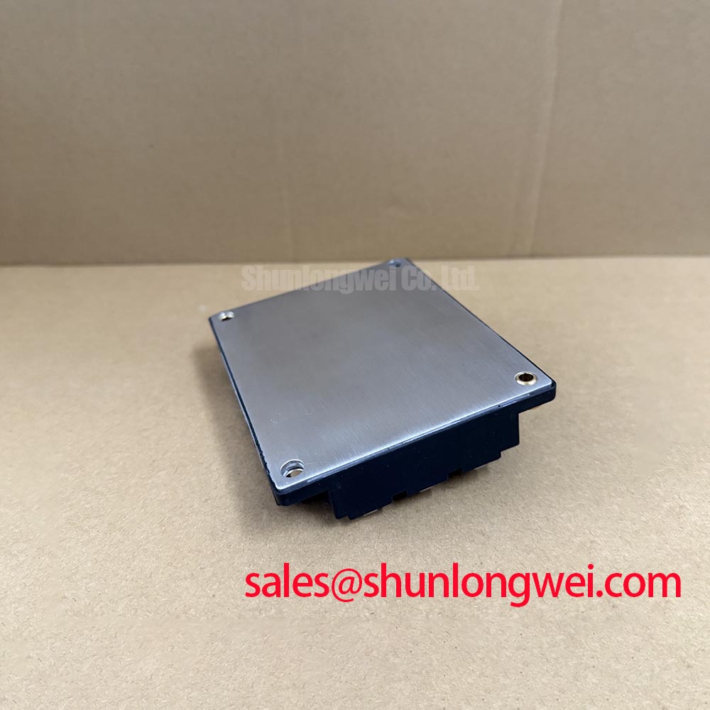
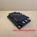
The Fuji Electric 7D75D-050EHR is a seven-pack PIM configuration rated at 500 V collector-emitter voltage and 75 A rated collector current. These are specification values for the component itself; the allowable operating point in a complete industrial inverter welder or medium-frequency induction-heating supply remains dependent on switching frequency, cooling conditions, current waveform, DC-link behavior, and the selected braking network.
When a motor drive or power conversion stage decelerates, the braking path must absorb returned energy without allowing the DC link to exceed the switching device voltage boundary. The braking IGBT, external ballast resistor, MOV network, wiring inductance, and control threshold should therefore be evaluated as one protection circuit. A resistor that is electrically suitable in steady operation may still create excessive thermal cycling during repeated acceleration and deceleration. Designers should verify pulse-energy capability, resistor temperature rise, enclosure airflow, and the actual DC-link waveform during the complete duty cycle.
For field replacement, first compare the failed circuit with a known-good phase or braking channel. Check for shorted power terminals, damaged gate wiring, loose busbar joints, discolored resistor connections, and cracked insulation around high-current paths. A cold resistance comparison is useful as a screening step, but it does not prove dynamic blocking capability. Any suspected device should be isolated from the gate driver and tested according to an approved power-semiconductor procedure before the DC link is energized.
Overvoltage suppression should be coordinated rather than added by guesswork. An MOV can help clamp transient energy, but its voltage rating, energy capability, repetition rate, leakage behavior, and location must match the DC-link architecture. Keep the high-current commutation loop compact and route the braking return path so that parasitic inductance does not increase turn-off overshoot. During commissioning, use a properly rated differential probe and verify the measured peak voltage against the module’s official 500 V VCES rating and the system engineer’s approved operating margin.
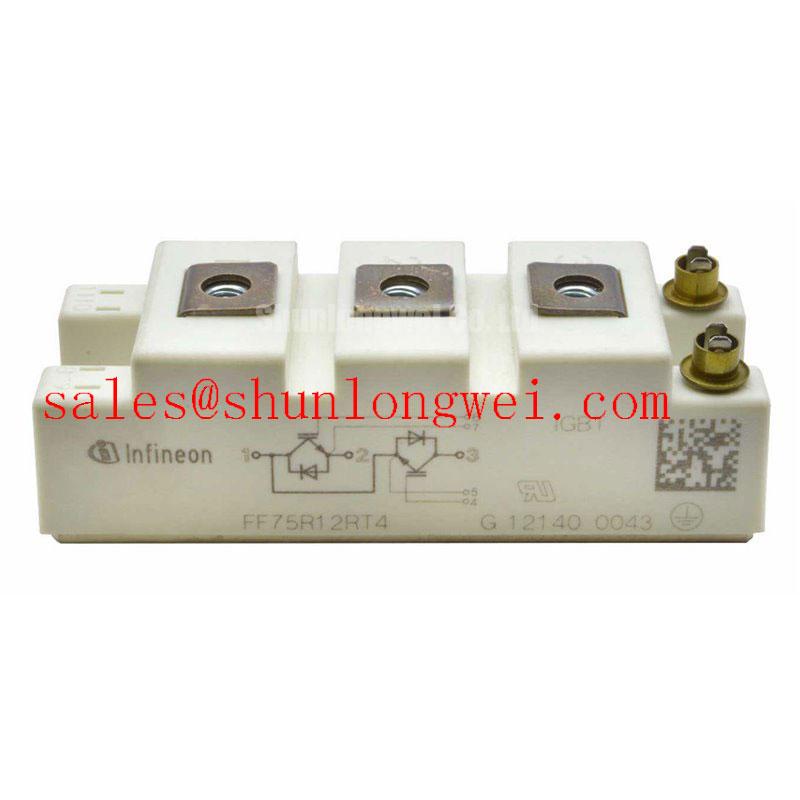
For a neutral comparison point, engineers reviewing a different Fuji Electric power-module topology may also examine 3MBI50SX-120-02. It should be assessed from its own datasheet, electrical configuration, terminal arrangement, and thermal requirements rather than treated as an automatic substitute for the 7D75D-050EHR.
7D75D-050EHR Thermal-Electrical Optimization: Optocoupler vs Digital Coreless Transformer Practical Tuning
The gate-drive interface must be checked as a system interface, not inferred from the power rating alone. The official data supplied for the 7D75D-050EHR identifies a gate-emitter threshold voltage of 6.0 to 8.0 V. This threshold is a conduction threshold reference, not a recommended gate-drive supply or a guaranteed turn-on command level. The integrator should verify the original driver documentation for gate voltage, peak source and sink current, isolation construction, desaturation implementation, and interlock behavior.
Optocouplers and coreless-transformer digital isolators respond differently to common-mode switching events. An optocoupler-based board should be checked for propagation-delay matching, aging-related timing drift, LED drive integrity, and collector-side pull-up behavior. A digital isolator should be checked for its specified common-mode transient immunity, supply bypass layout, reset state, and behavior during undervoltage or loss of input signal. If the application requires a reinforced isolation barrier or a particular CMTI performance level, those values must come from the driver manufacturer’s documentation and the complete assembly evaluation; they are not specifications of this IGBT module.
The 7D75D-050EHR has an official collector-emitter saturation voltage value of 2.1 V. A desaturation circuit may use the switching node behavior as part of short-circuit protection, but the sensing blanking period, fault threshold, propagation delay, and soft turn-off profile must be selected from the driver design and verified with the actual module and layout. The protection sequence should distinguish normal turn-on charging behavior from a genuine fault, then remove gate drive in a controlled manner that limits both current and inductive voltage overshoot.
During troubleshooting, observe the gate-to-emitter waveform directly at the module terminals rather than at the driver output connector. Compare turn-on delay, turn-off delay, plateau behavior, ringing, and the dead-time relationship between complementary channels. An unexpected pulse can arise from common-mode coupling, inadequate return-path control, driver supply disturbance, or a measurement reference problem. Confirm the signal with an isolated, bandwidth-appropriate measurement setup before changing gate components.
Where the power topology includes an upstream rectifier or complementary conversion stage, the 6MBI300U-120 can be reviewed as a related system-level device. Its inclusion does not establish electrical compatibility with the 7D75D-050EHR; voltage class, current path, switching role, control timing, and thermal design must be checked independently.
Preventing Spurious Faults: SCSOA Overcurrent Protection: Implementing Guidelines for 7D75D-050EHR
Short-circuit protection should be validated with the complete gate driver, busbar, load, and protection circuit in place. The published module data confirms the 75 A rated collector-current value, but this rating is not a short-circuit withstand specification. Short-circuit safe operating area, fault duration, repetition rate, junction temperature, and circuit inductance require the manufacturer’s applicable switching and protection data.
A practical protection review begins by checking where the fault is detected. Desaturation sensing, shunt-based detection, Hall sensing, or another method can produce different delays and noise sensitivity. The protection circuit should identify whether the fault is caused by a genuine load short, a saturated magnetic component, a gate-drive timing error, a failed freewheel path, or a measurement artifact. Engineers should verify the response time against the approved SCSOA data for the exact device revision rather than applying a generic microsecond limit.
Two-stage turn-off is a design consideration for reducing the electrical stress created when a high-current fault is interrupted. The first action can reduce gate drive in a controlled manner, followed by a defined fault-latch state that prevents an immediate restart. The actual gate resistance, current sink capability, fault blanking, and reset logic must be determined from the driver and switching-loop test results. The objective is to suppress excessive inductive overshoot while avoiding a turn-off response so slow that the module remains exposed to destructive fault energy.
When several devices or parallel current paths are used elsewhere in the system, positive temperature coefficient behavior may assist static current sharing, but it does not guarantee equal dynamic sharing. Busbar symmetry, gate-loop matching, emitter or source return impedance, driver timing, and thermal coupling should be compared between paths. A scope record taken at each gate and power terminal is more useful than assuming that equal nominal wiring produces equal transient current.
Fault investigation should include the resistor network, MOV condition, gate-driver supply rails, interlock logic, cooling interface, and recent changes to switching frequency or load profile. Check the module after isolation from external semiconductors, then compare its terminal behavior with the corresponding healthy channel. Do not reapply full DC-link voltage until the cause of the protective trip has been narrowed and the precharge, discharge, and emergency isolation functions have been tested.
7D75D-050EHR Thermal-Electrical Optimization: Active Miller Clamp Implementation Practical Tuning
High dv/dt at one switching device can couple through the opposing device’s Miller capacitance and produce an unintended gate excursion. An active Miller clamp can reduce this risk by providing a low-impedance discharge path while the commanded device is off. Whether that function is required depends on the gate-driver architecture, switching speed, layout, dead-time, and measured gate waveform; it is not an internal feature confirmed by the supplied 7D75D-050EHR specification data.
The first inspection point is the gate-to-emitter loop. Keep the driver return connected to the intended emitter reference, minimize the shared power-current path, and separate control wiring from high dv/dt copper where the mechanical design allows. Verify that the clamp activates only after the gate has reached its off-state and that it does not fight the normal turn-on command. Complementary-channel dead time should be established from measured switching behavior, device temperature, load current, and driver delay rather than copied from an unrelated module.
A negative gate bias may be considered in applications with severe switching transients, but the permitted gate-emitter voltage, driver supply arrangement, insulation coordination, and transient limits must be verified from the module and driver documentation. The 7D75D-050EHR official data supplied here specifies the threshold range and saturation voltage, but it does not authorize a particular positive or negative gate-bias value. Bench tuning should begin with a conservative driver configuration and proceed only after confirming the gate-emitter waveform under the highest relevant switching stress.
Gate dielectric reliability also deserves attention when a negative bias is used repeatedly. The discussion of Negative-Bias Temperature Instability provides useful background on how prolonged electrical and thermal stress can affect gate dielectric behavior in semiconductor structures. It should not be treated as a device-specific lifetime prediction for this Fuji Electric module.
For inverter welders and medium-frequency induction-heating supplies, inspect the clamp response with a differential probe at the module pins, then compare it with the driver’s fault and enable signals. Look for false turn-on, excessive ringing, unequal channel timing, and gate voltage collapse during a controlled load transition. The final acceptance decision should be based on measured peak gate voltage, collector-emitter overshoot, thermal behavior, and the approved limits for the complete converter.
⚡ Field Alert: Disconnect the DC link and confirm residual voltage is absent before inserting or removing gate-drive connectors, and follow the fastener and thermal-interface procedure specified for the actual heatsink assembly.
For broader repair references covering inverter, renewable-energy, electric-vehicle, and heavy-industry power stages, engineers can consult Industrial Applications while keeping the final electrical validation specific to the 7D75D-050EHR installation.
| Parameter | Symbol | Listed Value | Unit |
|---|---|---|---|
| Collector-emitter voltage | VCES | 500 | V |
| Rated collector current | IC | 75 | A |
| Collector-emitter saturation voltage | VCE(sat) | 2.1 | V |
| Gate-emitter threshold voltage | VGE(th) | 6.0 to 8.0 | V |
| Specified junction-temperature range | Tj | −40 to +150 | °C |
| Configuration | Type | 7-Pack PIM | Unit |
The listed electrical values are datasheet values; the applicable test conditions, rating conditions, and thermal limits govern their use in a complete application.