

Content last revised on September 11, 2026
7MBP100NA060-01 Thermal-Electrical Optimization: Auxiliary Emitter Return Trace Separation Practical Tuning
Start by tracing every control return from the gate driver to the installed module. In a high-current converter, a gate-drive return that shares copper, a connector path, or a long harness segment with the main emitter current can pick up voltage produced by changing current. That induced voltage can alter the gate-emitter voltage seen by the switching device, even when the driver output appears correct at its own terminals.
Design Consideration: where the original module terminal arrangement and circuit documentation provide a dedicated auxiliary emitter or control-return connection, route that return directly to the corresponding driver reference point rather than merging it into the main high-current emitter path. This separates the measurement reference from the power-current voltage drop and can help reduce gate-loop disturbance during switching. The exact terminal availability and function must be verified from the original equipment documentation for 7MBP100NA060-01; no terminal configuration should be inferred from the module family name alone.
During a fault investigation, inspect for a driver return conductor that has been moved during previous service, a loose low-current terminal, or a gate cable bundled tightly with a high-current conductor. Oscilloscope measurements should compare the gate-emitter waveform at the module-side connection with the driver-side waveform while observing the relevant switching node. Ringing, unexpected gate movement, or inconsistent switching behavior may indicate an impedance or reference-path issue, but the result should be compared with a known-good channel and the system schematic before assigning a cause.
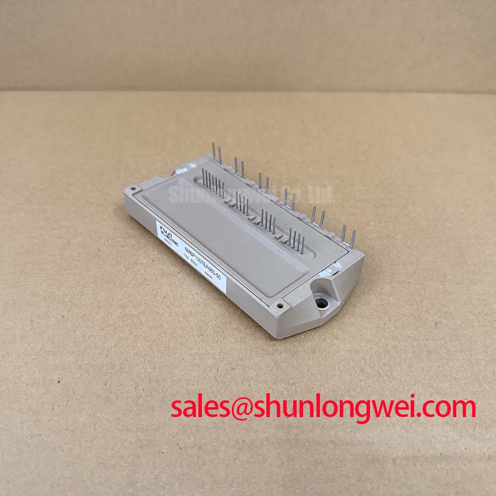
A unit with the same nominal voltage and current class does not automatically share mechanical fit, terminal mapping, control topology, or switching behavior. For a documented comparison reference, engineers can review the 6MBI100L-060 alongside the original drawings and mounting layout. This is a neutral reference point for evaluation, not a statement of interchangeability.
⚠️ Maintenance Note: Isolate and discharge the DC link before touching gate or power connections, then recheck terminal tightness and cooling-air paths after service work.
Plant maintenance should also include periodic checks for dust accumulation on the heatsink fins, blocked fan paths, aged thermal interface material, moisture ingress, and condensation risk after large temperature changes. These checks are general maintenance practices, not model-specific lifetime predictions. Recording contact-temperature trends and checking airflow condition can provide a more useful service baseline than relying on visual inspection alone.
7MBP100NA060-01 Thermal-Electrical Optimization: Dynamic Gate Impedance Control for Robust Practical Tuning
Gate impedance is a system-level control variable, not a fixed component value that can be prescribed from the module voltage and current ratings alone. It influences switching speed, driver peak current, voltage overshoot, electromagnetic emissions, and the susceptibility of an inactive switch to Miller-induced gate rise. The driver supply arrangement, isolation method, gate-loop geometry, DC-link placement, load type, and measured waveform margins all determine the final setting.
Design Consideration: when high switching-node voltage slew rate is present, designers commonly review whether the inactive gate is held with sufficient low impedance and whether the driver architecture includes an active Miller clamp. A negative off-bias supply is also evaluated in some gate-drive systems to increase immunity against unintended turn-on. The appropriate off-state bias and clamp behavior must be defined by the original driver design, the applicable device documentation, and bench validation; they cannot be assigned solely from the 600V, 100A module rating.
For service teams examining intermittent overcurrent trips, capture gate-emitter voltage, collector-emitter voltage, and current with measurement points referenced correctly to the power stage. A waveform that changes after tightening a terminal, replacing a gate harness, or restoring a short return path may reveal a layout-sensitive condition. Avoid interpreting a single waveform feature as proof of one failure mechanism. Check driver enable timing, isolated supply stability, connector contact quality, control-ground routing, and the condition of nearby snubber parts as related evidence.
The reverse recovery behavior of a freewheeling path can contribute to current transitions and radiated noise. Snubber networks can be evaluated as a Design Consideration when measured switching transients show excessive ringing, but capacitor type, placement, damping resistance, voltage capability, thermal loading, and pulse-current suitability must be selected by the system engineer. Place any effective suppression network close to the loop that generates the transient, then verify its impact with switching measurements rather than assuming that a larger component value is beneficial.
For background on gate-drive behavior and the reasoning behind negative off-state control approaches, see Evolution of Negative Off-Bias Gate Drive Circuits. This technical reference supports troubleshooting discussion but does not establish a mandatory gate-drive value for this module.
7MBP100NA060-01 Thermal-Electrical Optimization: Thermal Cycling Margins of Braking Systems Practical Tuning
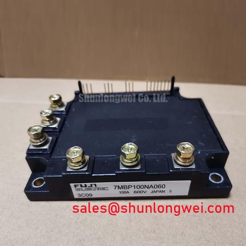
In inverter welder and induction-heating equipment, deceleration energy, load changes, and DC-link regulation must be understood from the equipment’s actual topology. A braking function may be handled by a dedicated external circuit, another section of the power assembly, an energy-return arrangement, or a resistor-based dissipation path. The presence, location, and rating of any braking function must be verified from the original schematic. The supplied product information identifies 7MBP100NA060-01 as a 600V, 100A module, but it does not establish an internal braking configuration.
Engineering Recommendation: where a braking transistor and resistor network are used in the host equipment, evaluate them as an energy-handling subsystem rather than by nominal module current alone. The required energy absorption depends on the driven load, operating sequence, DC-link control threshold, repetition pattern, resistor thermal path, and protection coordination. Engineers should review the original resistor assembly for discolored hardware, loose terminations, cracked insulation, reduced airflow, and abnormal heat transfer to adjacent wiring.
Thermal cycling is best managed through stable mechanical contact and repeatable cooling conditions. Before mounting a replacement module, clean the heatsink contact surface using an approved process, inspect it for burrs or localized damage, and apply the thermal interface material according to the original equipment procedure. Use the specified fastening sequence and torque from the equipment or module documentation. A distorted mounting surface or uneven clamp force can create localized temperature rise, but neither condition can be quantified without the relevant mechanical specification and thermal measurement.
In preventive maintenance, compare operating temperature trends between equivalent phases or channels where the machine architecture permits it. A rising difference may justify inspection of fan performance, heatsink cleanliness, thermal interface condition, current balance, and terminal resistance. It does not independently prove degradation inside the module. Keep records of ambient conditions and service changes so that a recurring thermal pattern can be separated from a temporary process load change.
Where the converter includes a separate front-end rectifier stage, its interaction with the DC link also matters during abnormal voltage events. The 6MBI100S-140 can be reviewed as a related power-device reference when checking documented rectifier or complementary-stage assemblies. Compatibility must remain subject to the original circuit, electrical ratings, insulation requirements, and mechanical layout.
7MBP100NA060-01 Thermal-Electrical Optimization: Planar Symmetrical Busbar Geometry Practical Tuning
Inspect the DC-link loop as a physical circuit, not only as a schematic. The path from the DC-link capacitor through the module and back to the capacitor carries rapid switching current. Long separated conductors, uneven parallel paths, loose laminated connections, or a capacitor placed remotely from the commutation loop can increase stray inductance. During turn-off, the resulting peak voltage follows the physical relationship that peak voltage rises above the DC-link voltage by stray inductance multiplied by the rate of current change. This is an Engineering Calculation principle, while the actual peak must be measured in the installed system.
Design Consideration: planar, closely coupled supply and return conductors are commonly used to minimize loop inductance and reduce radiated fields. Symmetry between parallel paths also matters because unequal geometry can shift current distribution and make one path appear thermally or electrically stressed first. The final geometry must accommodate insulation spacing, equipment clearances, service access, mechanical restraint, and the measured switching behavior of the complete converter.
When investigating overshoot or ringing, check the DC-link capacitor terminals, busbar hardware, module power connections, and any snubber assembly for signs of movement, heat discoloration, or compromised contact surfaces. Measure at the relevant module-side points using a probing method suitable for fast transients; long probe ground leads can create misleading ringing. Compare the waveform before and after any controlled layout correction, and confirm peak voltage remains within the system’s validated margin against the module’s 600V rating.
A capacitor added far from the switching loop may have limited influence on the highest-frequency transient because its connecting path becomes part of the loop. Conversely, a close suppression component can alter ringing and losses in ways that require thermal and waveform verification. For that reason, snubber selection, busbar geometry, gate timing, and protection thresholds should be validated together by the system engineer. This disciplined approach supports repair decisions without treating a generic layout practice as an official guaranteed characteristic of the module.