
Content last revised on October 27, 2026
Field Diagnostics & Commissioning: Mitigating Bolted Contact Oxidation in 7MBR25XKC120-50 Assemblies
With the DC link discharged and verified safe, identify the power terminals and gate connections of the 7MBR25XKC120-50 against the equipment schematic before making cold-state measurements. Separate module readings from parallel paths through the bus capacitors, braking circuit, and gate-driver board. Otherwise, a resistance or diode-mode result can describe the surrounding assembly rather than the semiconductor path under examination.
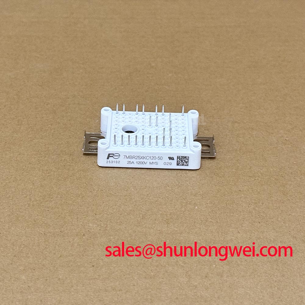
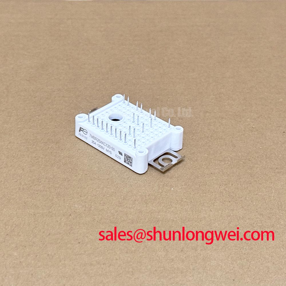
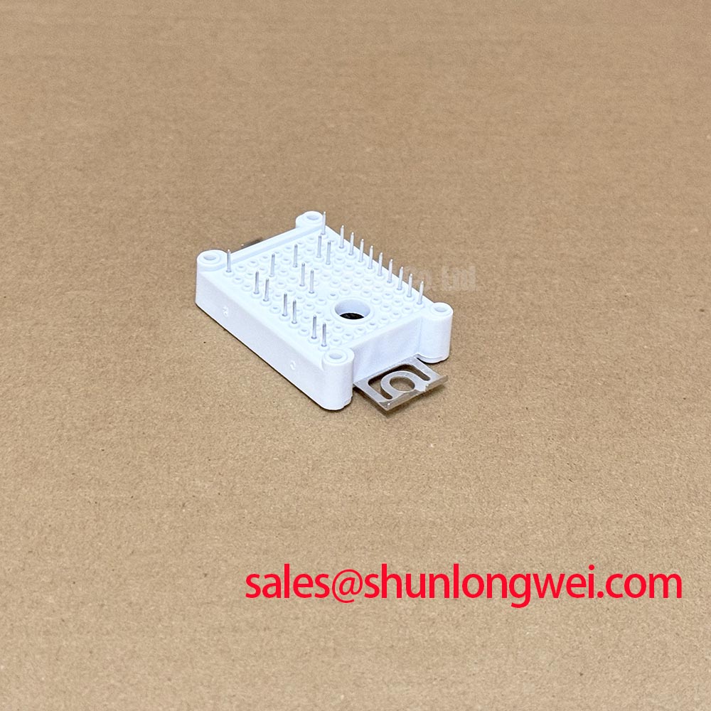
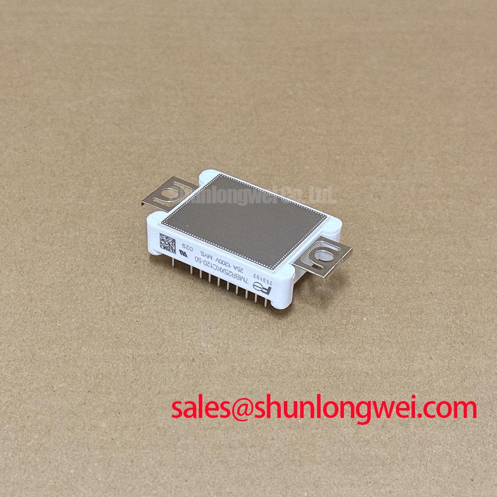
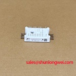
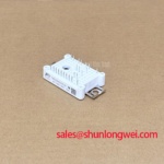
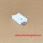
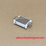
The Fuji Electric 7MBR25XKC120-50 is a 7th Gen X-Series power integrated module with a converter-inverter-brake topology incorporating seven IGBTs. It has a 1200 V collector-emitter voltage rating and a 25 A collector-current rating under the specified datasheet conditions. These identifiers establish the starting point for incoming inspection; they do not establish compatibility with an existing driver, mounting arrangement, or protection circuit.
Fuji Electric’s PIM Power Integrated Module 7-Pack overview provides the relevant product-family context. Treat the converter, inverter, and braking sections as distinct measurement paths when preparing an inspection record. Integration in one package does not make every terminal pair electrically equivalent, and a PIM designation alone does not establish integrated gate-drive or fault-protection functions.
Measure each accessible bolted power connection with a four-wire micro-ohmmeter, placing the sense probes across the joint rather than along the attached conductor. As a Design Consideration, this separates contact resistance from busbar resistance and helps distinguish a connection problem from semiconductor conduction losses. Record probe positions, joint temperature, instrument settings, and assembly condition so subsequent measurements remain comparable.
A repeatable comparison is more useful than an arbitrary universal micro-ohm acceptance limit. Compare equivalent connections with similar conductor geometry and temperature, then assess deviations against the equipment manufacturer’s acceptance procedure. Oxidation, contamination, uneven seating, conductor stress, and damaged contact surfaces can all contribute to an elevated reading. Cleaning or retightening should follow the approved assembly method rather than an assumed torque derived from the apparent screw size.
Thermographic inspection adds useful evidence after controlled energization. Compare corresponding terminals under comparable loading and account for surface emissivity, reflections, airflow, and viewing angle. A warmer joint warrants investigation, but the image alone does not identify oxidation as the cause. Correlate the thermal pattern with measured joint resistance, current distribution, and the mechanical condition of the connection.
For semiconductor screening, use the module circuit diagram to identify the expected diode conduction direction before applying the meter probes. Record diode-mode readings for corresponding inverter paths using the same instrument and temperature conditions. Differences can justify further investigation, but there is no universal handheld-meter forward-voltage threshold that independently certifies this module as serviceable. Gate-driver resistors and other connected circuitry should be accounted for before interpreting gate-to-emitter measurements.
💡 Bench Tip: Use ESD precautions and compare cold-state readings with a known-good unit under matching conditions, keeping the gate referenced according to the approved handling procedure.
Keep collector-emitter blocking capability separate from insulation withstand during acceptance checks. The 1200 V rating describes a semiconductor electrical limit, not a terminal-to-baseplate dielectric test voltage. An insulation test requires the manufacturer’s specified terminal grouping, test conditions, and acceptance criteria. Disconnect circuitry that is not intended to receive the test stress, and do not use a successful low-voltage resistance measurement as proof of dielectric integrity.
Before reassembly, inspect terminal seating, busbar alignment, enclosure spacing, and the condition of the mounting interface. As an Engineering Recommendation, conductors should meet the module without forcing the terminals into alignment. Preserve the equipment’s intended creepage and clearance paths, including around fasteners and conductor edges. Mechanical loading from a displaced busbar can compromise an otherwise acceptable electrical connection.
Transient Dynamics & Electrical Design: Negative Gate Bias vs Active Miller Clamping on 7MBR25XKC120-50
Capture the off-state gate-emitter waveform during complementary-device switching when investigating suspected parasitic turn-on. As a Design Consideration, collector-voltage transitions can couple displacement current into the gate circuit through Miller capacitance. Whether that disturbance produces unintended conduction depends on the gate discharge path, driver impedance, interconnect parasitics, and operating conditions—not on the nominal gate command alone.
Negative off-state bias and active Miller clamping address this disturbance differently. Negative bias increases the gate-voltage separation from turn-on, while an active clamp provides a local discharge path when its operating conditions are satisfied. Neither should be assigned a generic voltage or treated as an automatic upgrade. The driver’s output behavior, clamp engagement, gate-voltage limits, and supply sequencing must be evaluated together.
The technical article Evolution of Negative Off-Bias Gate Drive Circuits offers background for that comparison. For this module’s integration, the practical objective is to maintain a controlled off-state gate potential throughout switching and supply transitions. Inspect the gate return path and place measurements close to the relevant module terminals; a waveform captured only at the driver connector can conceal local ringing.
Dead time should be evaluated from the actual switching sequence rather than copied from another drive. As an Engineering Recommendation, compare command timing with gate waveforms and current behavior across the intended operating range. Propagation-delay differences, turn-off behavior, and driver-supply variation affect the required separation. Excessive dead time also changes output behavior, so the appropriate setting is a system-validation result rather than a fixed property of the 7MBR25XKC120-50.
Replacement assessment belongs alongside this gate-drive review because a shared manufacturer name does not establish electrical interchangeability. The 7MBI100U4E-120 can be included in a broader Fuji Electric component comparison, but it should not be treated as a drop-in replacement. The following comparison distinguishes established product facts from items requiring a separate technical match.
| Selection checkpoint | 7MBR25XKC120-50 | 7MBI100U4E-120 comparison requirement |
|---|---|---|
| Manufacturer | Fuji Electric | Fuji Electric |
| Collector-emitter voltage | 1200 V — specified rating | Consult datasheet |
| Collector current | 25 A — under specified datasheet conditions | Consult datasheet and rating conditions |
| Circuit configuration | Converter-inverter-brake PIM with seven IGBTs | Compare internal circuit and terminal functions |
| Series and package | 7th Gen X-Series PIM; consult package outline | Compare technology, outline, and mounting interfaces |
| Replacement decision | Reference device for this assessment | No drop-in equivalence established |
Fuji Electric’s High-Speed Discrete IGBT overview describes a separate device category, not an interchangeable package alternative. Moving between discrete devices and an integrated power module changes interconnections, mechanical interfaces, and the protection implementation. Component selection must preserve the required circuit functions rather than match voltage and current labels alone.
When evaluating this PIM for a compact industrial inverter or high-speed CNC spindle drive, include the motor cable and output network in commissioning tests. As a Design Consideration, cable reflections can increase motor-terminal voltage stress; they are distinct from DC-link switching overshoot at the module. Assess cable length, switching edge behavior, motor insulation requirements, and any proposed output filter together. Filtering decisions should follow measured system behavior rather than an assumed universal reflection multiplier.
Preventing Spurious Faults: High-Speed Semiconductor Fuse I²t Guidelines for 7MBR25XKC120-50
Compare a candidate semiconductor fuse’s total-clearing characteristics with the actual fault circuit before accepting it as protection for the 7MBR25XKC120-50 assembly. As a Design Consideration, pre-arcing I²t describes only the interval before the fuse element melts; total-clearing I²t also includes the arcing interval. Confusing those quantities can produce an optimistic coordination assessment.
Protection evaluation must distinguish the converter diodes, inverter IGBTs, and braking path. A withstand characteristic associated with one semiconductor section cannot automatically be transferred to another. Likewise, an IGBT short-circuit withstand time under specified gate-drive conditions is not interchangeable with a diode surge-current rating or a fuse let-through characteristic. Apply each manufacturer curve only to the device section and conditions it describes.
DC interruption capability matters because the fault circuit must extinguish current after the fuse element opens. Review the fuse’s voltage rating, interrupting capacity, circuit time-constant conditions, and the equipment’s prospective fault current. DC-link capacitors can contribute stored energy through paths that differ from the incoming supply path. A fuse location should therefore be assessed against the schematic and physical current loop, not just its accessibility in the enclosure.
Fast electronic protection and fuses perform different jobs. As an Engineering Recommendation, verify the gate driver’s fault detection, blanking behavior, shutdown response, and controlled turn-off using the equipment’s approved test procedure. A fuse cannot be assumed to prevent IGBT damage during every rapidly developing fault, and successful fuse coordination alone does not establish containment against package rupture.
For unexplained trips, preserve the fault record before changing protection settings. Compare the reported event with DC-link behavior, gate-driver supply stability, current-sensor output, and the operating transition that preceded it. Switching-related measurement interference, supply disturbances, genuine overcurrent, and unintended conduction require different corrective actions. Raising a threshold without identifying the initiating condition can conceal useful diagnostic evidence.
Inspect fuse holders and adjacent connections as part of that investigation. Local heating can arise from contact resistance or operating conditions as well as fuse selection. Check conductor support, cooling exposure, and separation from sensitive gate wiring. After corrective work, repeat the approved startup and load sequence while observing terminal temperatures and protection signals, then retain the measurement setup and results with the equipment service record.