Content last revised on September 10, 2026
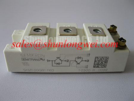
Infineon BSM200GAR120DN2 IGBT Power Module
Decoding Voltage Ratings and Thermal Efficiency for Heavy Industrial Motors
The Infineon BSM200GAR120DN2 is a high-performance single-switch IGBT power module equipped with a reverse chopper configuration and an integrated fast free-wheeling diode. Operating at a maximum VCES of 1200V and a continuous collector current IC of 200A (at TC = 80°C; 300A at TC = 25°C), this module is structured to deliver dependable switching behavior in demanding industrial environments.
With an extremely low junction-to-case thermal resistance RthJC ≤ 0.08 K/W for the IGBT chip and a power dissipation rating Ptot of 1550W, the device maintains tight thermal management under high current switching operations. Its baseplate-insulated package ensures robust electrical isolation up to 2500V AC, simplifying chassis mounting and heat sink layout in heavy-duty converters.
- Low Thermal Resistance: High-efficiency heat transfer with RthJC ≤ 0.08 K/W to extend operating lifetime.
- High Surge Margin: Handles pulsed collector currents up to 600A for inductive load transients.
For 1200V motor drive applications requiring minimal thermal overhead and fast switching response, the BSM200GAR120DN2 offers an optimized balance of low conduction losses and switching endurance.
Key Parameter Overview
Core Specifications and Electrical Limits
To assist power design engineers in evaluating system margins, driver requirements, and thermal constraints, the table below outlines the primary operating limits and static characteristics of the BSM200GAR120DN2.
| Parameter | Symbol | Test Conditions / Value | Unit |
|---|---|---|---|
| Collector-Emitter Voltage | VCES | Tj = 25°C: 1200 | V |
| DC Collector Current | IC | TC = 80°C: 200 / TC = 25°C: 300 | A |
| Pulsed Collector Current | ICpuls | TC = 80°C, tp = 1ms: 600 | A |
| Total Power Dissipation | Ptot | TC = 25°C, per IGBT: 1550 | W |
| Collector-Emitter Saturation Voltage | VCE(sat) | VGE = 15V, IC = 200A, Tj = 25°C: 2.5 (typ) / 3.1 (max) | V |
| Gate-Emitter Threshold Voltage | VGE(th) | VGE = VCE, IC = 8mA: 4.5 to 6.5 | V |
| Thermal Resistance (IGBT Junction to Case) | RthJC | Per IGBT: ≤ 0.08 | K/W |
| Thermal Resistance (Diode Junction to Case) | RthJCD | Per Diode: ≤ 0.15 | K/W |
| Insulation Test Voltage | VISOL | t = 1 min, RMS: 2500 | V |
Download the BSM200GAR120DN2 datasheet for detailed specifications and performance curves.
Application Scenarios & Value
Targeted Deployment in Motor Control and Dynamic Braking
Engineers designing high-power motor control units frequently encounter severe transient currents and localized heat spikes during acceleration and deceleration cycles. The BSM200GAR120DN2 addresses these power stage challenges through its low saturation voltage VCE(sat) of 2.5V and high peak current carrying capability (ICpuls up to 600A). In dynamic braking circuits or reverse chopper configurations, the integrated fast free-wheeling diode safely recirculates inductive energy back to the DC bus without inducing damaging voltage spikes across the collector junction.
Consider an industrial Variable Frequency Drive (VFD) operating off a 480V or 690V AC line grid. High ambient temperatures inside industrial cabinets can significantly restrict heatsink dimensions. Because the BSM200GAR120DN2 features an RthJC of ≤ 0.08 K/W, thermal transfer from the semiconductor junction to the heatsink is exceptionally fast. Think of this thermal barrier as a wide, unimpeded highway for heat: energy generated inside the tiny silicon die flows outwards rapidly into the cooling system, guarding the junction against exceeding its 150°C maximum limit.
For systems with different topological needs or current demands, related alternatives such as the BSM300GA120DN2 provide higher current capacity in a single-switch layout, whereas the BSM200GB120DN2 offers a dual half-bridge configuration for full-bridge inverter stages.
Frequently Asked Questions
How does the RthJC rating of ≤ 0.08 K/W influence heatsink selection?
A lower thermal resistance between the IGBT junction and the module case allows heat to dissipate quickly, which reduces the required surface area and thermal mass of the external heatsink while preserving a safe operating temperature.
What is the primary benefit of the module's reverse chopper (GAR) topology?
The GAR topology integrates a chopper transistor with an anti-parallel diode configuration tailored for braking and power recovery units, minimizing external component count and stray inductance in DC bus protection circuits.
What gate driver requirements are necessary for driving the BSM200GAR120DN2 reliably?
The driver should supply a nominal gate voltage VGE of +15V for optimal conduction, alongside a recommended negative bias (e.g., -5V to -15V) during turn-off to prevent parasitic turn-on caused by high dv/dt noise.