Content last revised on October 13, 2026
CC1140 Operational Boundaries: Evaluating Critical Rate of Rise of Off-State Voltage Limits
Trace the installed snubber connections before changing resistance, capacitance, or reactor arrangements. As a Design Consideration, rapid off-state voltage changes can produce displacement current in a thyristor structure and contribute to unintended triggering. The relevant comparison is between the measured terminal waveform and the device’s specified critical voltage rise rate under its stated temperature and gate conditions.
For a thyristor position, inspect the RC snubber for damaged connections and changed component characteristics. Evaluate resistance against damping and pulse dissipation requirements, and capacitance against transient suppression and discharge current. If the equipment includes a series saturable reactor, assess its current rise control using the original circuit requirements. Component values remain system-dependent; increasing snubber capacitance without assessing discharge current can change the turn-on stress.
A separate gate-drive check helps distinguish terminal-voltage effects from unwanted control pulses. As a Design Consideration, examine the installed optocoupler or digital isolator’s common-mode transient immunity against the actual common-mode waveform, then observe the receiving-side signal and gate reference. This concerns the external driver, not a claimed CC1140 feature. Where an MOV is fitted, assess its clamping behavior together with snubber response and repetitive energy exposure.
Field Alert: Restore terminal and mounting fasteners to the applicable manufacturer instructions, and do not substitute a generic torque value for the specified joint requirement.
CC1140 Operational Boundaries: Evaluating Non-Repetitive Surge On-State Current Limits
Match the surge waveform and initial junction temperature to the non-repetitive surge rating before accepting a replacement. A sinusoidal 10 ms half-cycle is a relevant datasheet test condition to check, not an established CC1140 rating here. The surge assessment also needs the specified conditions for reverse-voltage reapplication; surviving a current pulse alone does not establish readiness for the following blocking interval.
For semiconductor fuse coordination, compare the fuse manufacturer’s total clearing I²t at the actual prospective fault current and circuit voltage with the module’s applicable withstand conditions. Include peak let-through current and interruption behavior. A comparison based only on fuse current rating misses the energy delivered during clearing, while an I²t comparison alone does not demonstrate complete short-circuit protection.
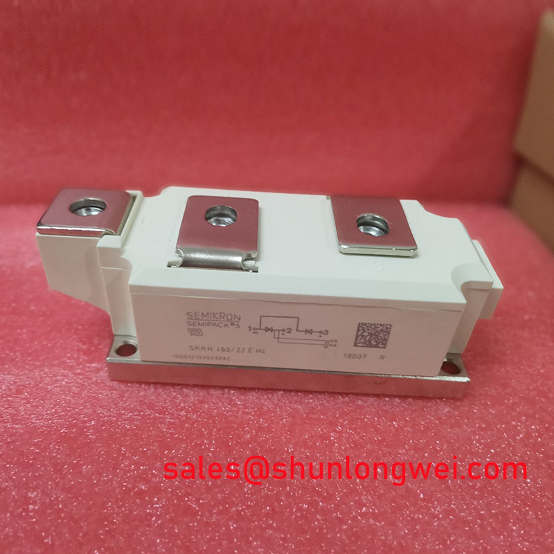
The following comparison separates supplied product descriptors from the evidence needed for substitution. UFB200FA40 is another part to examine during a replacement search, not an established compatible substitute.
| Replacement criterion | CC1140 | UFB200FA40 |
|---|---|---|
| Product identification | Diode/Thyristor Module | Separate model requiring circuit comparison |
| Package description | Isolated Module | Consult datasheet |
| Voltage and current limits | Consult datasheet; supplied descriptors contain no numerical ratings | Consult datasheet |
| Surge, fuse coordination, and terminal arrangement | Consult datasheet and equipment schematic | Consult datasheet and compare with the original position |
When evaluating a grid-tied static var compensator or thyristor-switched capacitor assembly, designers should verify branch topology, blocking polarity, gate requirements where applicable, and mechanical fit. Matching the enclosure alone is insufficient for acceptance.
CC1140 Thermal-Electrical Optimization: Diode Peak Reverse Recovery Current and Practical Tuning
Observe current reversal and terminal overshoot in the actual commutation path before attributing heating to diode reverse recovery. As a Design Consideration, peak reverse recovery current, recovery time, and recovery softness depend on test conditions, including forward current, current fall rate, and junction temperature. Recovery time alone does not define softness; compare the waveform shape and any manufacturer-defined softness parameter.
Use appropriately rated measurement equipment and account for probe-induced artifacts. Where the circuit includes a diode path, compare its measured recovery behavior with the corresponding device specification. The Shindengen power semiconductor resources and Mitsubishi Electric diode module lineup provide relevant manufacturer context, without establishing CC1140-specific recovery values.
For thermal assessment, combine pulse losses with the applicable transient thermal impedance data and measured case conditions. Inspect the mounting interface for flatness, contamination, and uneven contact. If devices operate in parallel, assess static and dynamic current sharing rather than assuming a favorable temperature coefficient. The Power Electronics Masterclass offers broader selection context; replacement acceptance should retain measured waveforms, thermal conditions, fuse coordination evidence, and the restored connection record.