

Content last revised on September 26, 2026
Benchtop Waveform Tuning: Mitigating Stress via Thermal Interface Material Thickness Uniformity on CM421655
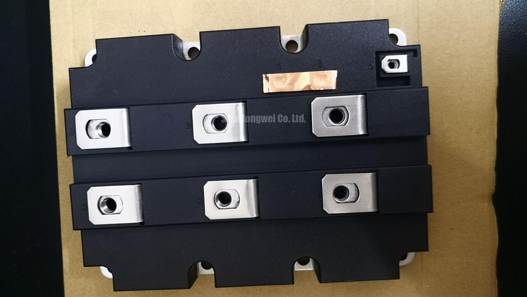
Start the mechanical inspection with the cooling interface rather than applying gate pulses. The baseplate and heatsink should be clean, flat, and free from burrs, embedded particles, or old thermal compound. A thermal interface material layer should be continuous and as uniform as the selected compound and installation method allow. The requested working range of approximately 50 to 100 µm may be used only as a Design Consideration for a suitable interface process, not as an official CM421655 specification. The actual thickness should be determined by the compound supplier, surface flatness, clamping system, and thermal validation results.
Excess compound can increase thermal resistance and migrate toward terminals, while insufficient coverage can leave air pockets below the baseplate. Apply the material in a controlled pattern, then inspect the contact imprint after a trial assembly where the production process permits. A curved or uneven baseplate should not be corrected by adding a thick local layer of compound. The mechanical condition should be measured and corrected through the approved heatsink preparation or clamping method.
Use a sequential tightening pattern so the baseplate settles progressively instead of being pulled down from one corner. The correct fastener type, washer arrangement, spring or disc-spring loading, and torque must come from the Mitsubishi Electric mechanical documentation or the equipment manufacturer’s assembly specification. Do not treat a generic M5 torque value as an official requirement for this module. After installation, check the contact pattern, terminal alignment, and heatsink seating before applying bus voltage.
For waveform work, begin with a low-energy commissioning condition and observe collector-emitter voltage, gate-emitter voltage, and current transitions with suitable isolated measurement equipment. If turn-off overshoot or ringing is observed, review commutation-loop inductance, probe connection, gate resistance, and the clamping network together. Changing the external gate resistor alone may mask a layout or measurement problem. Any final operating point should be established by the system designer after checking peak voltage and thermal behavior against the complete converter limits.
⚠️ Maintenance Note: Monitor the temperature rise across the module-to-heatsink interface during scheduled service and recheck the cooling path after fan, filter, or ductwork maintenance.
Field Diagnostics & Commissioning: Using Galvanic Gate Drive Isolation in CM421655 Topologies
The supplied product data identifies the CM421655 as a high-current, high-voltage module, but it does not provide an isolation rating, common-mode transient immunity value, gate charge, or recommended gate-drive current in the available specification set. Those values must be confirmed from the applicable Mitsubishi Electric technical documentation. Mitsubishi Electric’s Power Semiconductors and High-Power Modules resource is an appropriate manufacturer reference point for product-family documentation.
During commissioning, verify the isolation barrier between the control electronics and the power-side switching circuit with the approved test method for the complete gate-driver assembly. A reinforced isolation architecture and high common-mode transient immunity may be required by the system, but the relevant withstand and CMTI values are system and driver specifications that must not be assigned to CM421655 without documentary support. Check the isolation barrier, cable routing, shield termination, and local supply decoupling as one signal path.
The gate driver should provide controlled source and sink current suitable for the selected switching speed and gate-charge behavior. The correct peak current is an Engineering Recommendation determined from the verified gate-charge data, driver voltage, switching frequency, thermal limits, and acceptable voltage overshoot. External gate resistance should be selected as a tuning element: increase damping when ringing is confirmed, then verify switching loss and junction temperature; reduce impedance only after the measured waveform and protection margins support the change.
Bootstrap arrangements require particular care when the driver supply is refreshed by high-frequency charging and discharging. Confirm that the capacitor voltage remains within the gate-driver operating window during the full pulse sequence, and verify diode reverse-recovery behavior against the switching loop. If the original equipment uses an isolated auxiliary supply rather than a bootstrap supply, the replacement design should preserve the documented power architecture instead of assuming interchangeability.
In a traction inverter evaluation, the CM421655 may be considered alongside the rectification and DC-link topology. The related CM100DY-12E can be reviewed as a separate peripheral or complementary-stage reference, but compatibility depends on voltage coordination, current sharing, mechanical interfaces, drive timing, and the original circuit documentation.
Assembly Integrity & Layout Architecture: Implementing PCB Gate Loop Layout Symmetry for CM421655
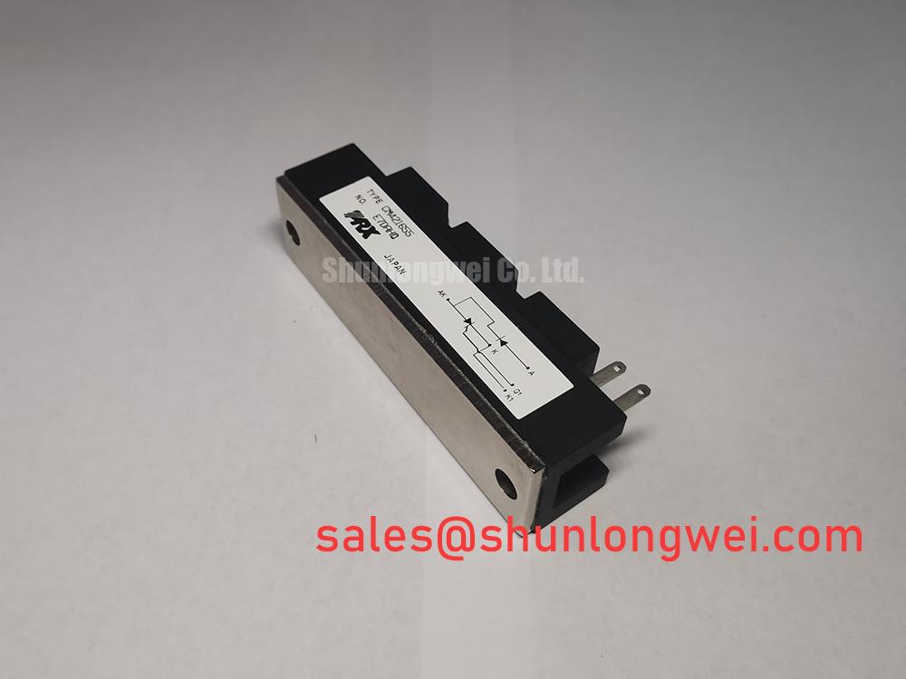
Keep the gate-drive loop compact and physically separated from the high-current commutation path. The control return should follow the intended gate-emitter reference rather than sharing an uncontrolled section of the main emitter conductor. Where the module provides an auxiliary control return, the integrator should verify its terminal definition from the original pinout documentation before assigning it a Kelvin function. No terminal role should be inferred only from the package appearance.
Symmetry between parallel switching paths is a Design Consideration when several devices or module sections operate together. Match conductor length, width, return geometry, and connector arrangement as far as the mechanical design permits. Unequal parasitic inductance can produce different gate-emitter transients, which may appear as timing mismatch, ringing, or irregular current distribution. Confirm the behavior with differential probes and current measurement rather than treating one waveform symptom as proof of a single failed component.
Maintain practical clearance around high-voltage copper, gate-driver connectors, and monitoring points according to the applicable insulation coordination standard and the assembled system’s working-voltage, pollution, altitude, and enclosure conditions. The CM421655 rating of 2750.0 V is an official product parameter, not a complete PCB creepage or clearance instruction. Those distances must be calculated and verified for the finished assembly.
For high-speed rail or heavy freight locomotive traction-inverter evaluation, inspect the mechanical interface after transport and vibration exposure. Check terminal clamping, busbar alignment, support points, and the condition of the thermal interface. A module can show acceptable static electrical behavior while a loosened busbar or uneven clamping arrangement creates intermittent switching stress during load changes.
Engineers comparing a related Mitsubishi Electric module can review CM300DXDX1-24A as a separate reference. It should not be treated as a direct substitute unless the electrical ratings, gate requirements, physical mounting, thermal path, protection coordination, and control timing have all been verified against the original equipment design.
The broader principles of substrate contact, thermal spreading, and cooling architecture are discussed in The Advanced Thermal Management Revolution. That technical background can support maintenance planning, but the final assembly method remains dependent on the actual module, heatsink, interface material, and converter structure.
CM421655 Circuit Protection & Reliability: Calibrating High-Speed Fault Management and VCE Desaturation
Protection design should begin by confirming whether the existing gate driver uses VCE desaturation detection, a current-sensing path, a shunt, a Hall sensor, or another fault method. The supplied CM421655 parameters do not specify a short-circuit withstand time, a type-I or type-II short-circuit limit, a desaturation blanking interval, or a required soft turn-off profile. Values such as detection below 10 µs therefore require verification from the applicable device documentation and the complete gate-driver design rather than being presented as CM421655 factory specifications.
A desaturation circuit should distinguish a genuine overcurrent event from diode recovery, switching noise, probe coupling, and normal voltage transition. The sensing diode, filter, blanking function, and fault latch must be evaluated under the actual DC-link voltage and switching conditions. If a fault is confirmed, a two-stage soft turn-off strategy may help limit the interaction between stored current and stray inductance, but the timing and gate-voltage trajectory must be tuned by the system engineer through controlled testing.
Coordinate the desaturation response with the DC-link clamp network. MOVs, active clamps, snubbers, and other overvoltage elements should be selected for the converter’s energy, repetition rate, voltage class, and fault behavior. A MOV is not a substitute for minimizing the commutation loop or validating the peak collector-emitter voltage. The complete network should be checked for clamping level, thermal loading, aging behavior, and interaction with the switching waveform.
Dead-time and interlock logic should prevent simultaneous conduction commands while allowing for driver propagation delay, turn-off behavior, and the power circuit’s recovery characteristics. A short, controlled buffer interval may be suitable, but its value is system-determined and must be validated with the actual driver and load. During fault testing, record gate signals on both switching channels, the DC-link voltage, collector-emitter voltage, and the fault output so that protection timing can be correlated without relying on a single symptom.
For a CM421655 replacement assessment, final release should follow documented checks of voltage rating, current rating, thermal contact, gate-drive compatibility, isolation, protection response, and mechanical integrity. The official identification data remains 2750.0 V, 4216.0 A, and Module package; all additional application limits require confirmation from the relevant Mitsubishi Electric and equipment documentation.