

Content last revised on November 8, 2026
Toshiba MG150Q2YS50 Overview and Initial Checks
Isolate the DC link, verify that stored energy has discharged, and disconnect the gate driver before checking the MG150Q2YS50 for collector-to-emitter shorts or abnormal gate-path impedance. Compare readings with an equivalent disconnected phase leg using the same meter polarity; connected snubbers, discharge resistors, and driver circuitry can otherwise obscure the result. A cold resistance check supports initial fault screening, but it does not establish switching performance under load.
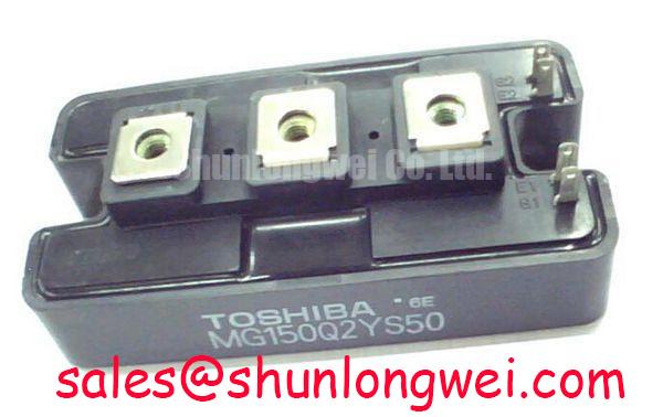
The Toshiba MG150Q2YS50 is an IGBT Module with a dual-IGBT half-bridge configuration. Its primary ratings are Collector-Emitter Voltage (Vces): 1200.0 V and Continuous Collector Current (Ic): 150.0 A. These official specification ratings identify the electrical class; operating current still depends on case temperature, switching losses, and the equipment cooling arrangement.
Official Specification: Manufacturer: Toshiba; Part Number: MG150Q2YS50; Package: Toshiba Module; Configuration / Topology: IGBT Power Stage. For replacement work, retain the original equipment schematic and terminal drawing alongside the module: matching the part designation is only the first compatibility check.
Transient Dynamics & Electrical Design: Derating Guidelines and Parameter Mismatch on MG150Q2YS50
Compare gate-loop routing and emitter return connections before attributing uneven phase heating to the MG150Q2YS50 itself. As a Design Consideration, unequal gate-path impedance can produce different switching delays even when power devices share the same designation. Check driver connectors, resistor joints, return-path continuity, and routing changes introduced during previous repairs. Measure gate voltage relative to the corresponding emitter connection rather than a remote control-board ground.
For parallel-device arrangements, distinguish static current sharing from switching balance. A positive temperature coefficient of collector-emitter saturation voltage can support static sharing only within the operating region where the device characteristics establish that behavior. It should not be assumed across the entire load range or treated as a verified MG150Q2YS50 characteristic without the relevant curves. Dynamic sharing instead depends strongly on gate-drive matching, power-loop geometry, and connection inductance.
As an Engineering Recommendation, compare collector current and gate waveforms at equivalent operating points while monitoring case temperatures. A hotter position can reflect unequal conduction, cooling contact, or switching energy; temperature alone cannot distinguish these mechanisms. Preserve symmetrical power connections where devices operate in parallel, and investigate unequal voltage drops across external joints before changing gate resistance.
Mechanical checks belong in this assessment because poor thermal contact changes the operating point being compared. Inspect the mounting surface for distortion, displaced interface material, and contamination around the baseplate. Follow the applicable assembly instructions for flatness, interface material, tightening sequence, and torque. Field Alert: Never compensate for a poor thermal interface by increasing mounting torque beyond the specified assembly limit.
At the terminals, retain the equipment’s designed creepage and clearance paths. Repositioned busbars, protruding hardware, conductive debris, or damaged insulating barriers can compromise those paths. As a Design Consideration, any layout change requires an insulation-coordination assessment against working voltage, pollution conditions, and the applicable equipment standard rather than a generic spacing rule.
MG150Q2YS50 Operational Boundaries: Commutation and Voltage-Spike Mitigation
Capture the commutating current and collector-emitter voltage together when investigating overshoot near the opposite switch’s turn-on transition. In a half-bridge, reverse recovery of the freewheeling path can contribute to current peaks and ringing. As a Design Consideration, separate reverse-recovery behavior from simultaneous conduction and probe-induced artifacts before adjusting the driver.
Peak reverse-recovery current and recovery abruptness depend on operating conditions, including preceding current, temperature, and commutation rate. The ROHM IGBT and intelligent-module technical resources provide broader device-technology context; their product characteristics do not establish Toshiba module limits. For this repair, evaluate the actual installed switching pair and its freewheeling path.
Gate-resistance changes and RC snubbers are system-level tuning measures, not automatic remedies. As an Engineering Recommendation, assess turn-on slew rate against recovery current, switching loss, and ringing before changing resistance. Snubber selection should account for measured oscillation, repetitive energy, resistor heating, and capacitor pulse capability. Reduced ringing on an oscilloscope does not independently demonstrate equipment-level EMC compliance.
Check complementary gate commands at the device terminals, including propagation-delay differences and turn-off tail behavior. Dead time should prevent overlap across the intended temperature and load range without creating unnecessary diode conduction. Verify interlock behavior during missing commands, driver undervoltage, and restart; software timing alone does not reveal every hardware fault path.
When reviewing replacement candidates, treat MG300Q2YS45 as a comparison item rather than an established interchangeable part. The following checks keep the procurement discussion tied to electrical and mechanical compatibility.
| Compatibility item | MG150Q2YS50 | MG300Q2YS45 comparison requirement |
|---|---|---|
| Manufacturer | Toshiba | Confirm manufacturer documentation |
| Collector-Emitter Voltage (Vces) | 1200.0 V | Consult Datasheet |
| Continuous Collector Current (Ic) | 150.0 A | Consult Datasheet |
| Package | Toshiba Module | Compare outline, terminal positions, and mounting |
| Configuration / Topology | IGBT Power Stage; dual-IGBT half-bridge | Compare circuit diagram and terminal assignments |
| Dynamic compatibility | Evaluate with installed driver and commutation circuit | Compare gate requirements, switching behavior, and thermal characteristics |
MG150Q2YS50 Operational Boundaries: Evaluating Turn-Off di/dt-Induced Peak Voltage, Clamping, and Limits
Inspect the complete commutation loop before adding a clamp across the MG150Q2YS50. As an Engineering Calculation, the simplified relationship Vpeak ≈ VDC + Lσ × |di/dt| explains why connection inductance raises turn-off voltage; actual waveforms also include recovery, capacitance, and ringing effects. Use measurements at the module terminals to establish the peak rather than estimating it from DC-link voltage alone.
As a Design Consideration, overlapping outgoing and return conductors can reduce commutation-loop inductance when insulation and assembly constraints permit. Keep local DC-link connections compact and preserve balanced geometry where branches operate together. The acceptable geometry is determined by measured switching stress, dielectric requirements, and mechanical tolerances—not an arbitrary inductance target.
Assess a clamp or snubber over repetitive operation, not just a single clean switching trace. Its voltage behavior, pulse-energy handling, thermal rise, and connection inductance all matter. An altered turn-off resistor can change both overshoot and switching dissipation, so compare electrical waveforms with thermal behavior after each controlled adjustment. Use appropriately rated differential probes and minimize measurement-loop pickup.
Trace the surrounding power-stage architecture before assigning a fault to one module. Where a service bill of materials includes MG200J2YS45 elsewhere in the converter, identify its actual circuit role from the schematic; its designation alone does not establish a rectifier function or compatibility with MG150Q2YS50. Upstream precharge faults and DC-link connection problems can affect the switching stage without originating inside it.
The application discussion in The Power Behind a Perfect Elevator Ride offers additional inverter context, not an acceptance standard for this module. Repair acceptance should remain tied to equipment service criteria and recorded voltage, current, and temperature measurements.
MG150Q2YS50 Thermal-Electrical Optimization: Driver and Power-Stage Start-Up Inrush Mitigation
Verify that the driver supplies and undervoltage interlocks establish a controlled off state before enabling the high-voltage DC link. As a Design Consideration, any negative gate bias must follow the approved driver design and device gate limits; it is not a substitute for reliable command inhibition. Observe startup and shutdown at the gate terminals, including auxiliary-supply collapse and interrupted power.
Separate DC-link charging inrush from unintended semiconductor conduction. Check precharge operation, bypass-contactor sequencing, and controller enable conditions against the equipment schematic. A startup current surge can involve several interacting paths, so correlate current with contactor state, bus voltage, and gate commands rather than assuming a failed module from the surge alone.
For commercial string inverter or micro-grid energy-storage compatibility assessment, designers should verify DC-link conditions, bidirectional operating requirements, cooling capacity, and protection coordination. As an Engineering Recommendation, evaluate pulse heating using the applicable transient thermal-impedance curves and loss profile. Case temperature alone cannot establish peak junction temperature during short load excursions.
Coordinate semiconductor fuses with the equipment’s prospective fault current and documented protection strategy. Fuse I²t describes let-through stress, but does not by itself establish IGBT short-circuit survival or containment. Confirm driver fault detection, controlled shutdown, and the module’s applicable short-circuit limits before relying on coordinated protection. After reassembly, verify thermal-interface contact and repeat startup checks under the equipment’s controlled commissioning procedure, recording gate behavior and bus-current response before increasing load.