Content last revised on October 17, 2026
Benchtop Waveform Tuning: Firing Delay Angle Assessment Around DD104N16
Isolate the rectifier from its supply, verify that stored energy has discharged, and compare forward and reverse diode readings across the disconnected power terminals before reconnecting a DD104N16. Parallel circuit paths can distort meter readings, so investigate an unexpected result with the module electrically separated from surrounding components. Record terminal orientation and inspect the mounting surface, terminal hardware, and insulating surfaces before disturbing the assembly.
The Infineon DD104N16 is a Diode Module with a specified reverse voltage rating of 1600 V and a rated average forward current of 104 A under the specified datasheet conditions, in a PowerBlock Module package. For replacement assessment, match the circuit arrangement, terminal connections, mechanical drawing, and thermal conditions alongside those ratings.
Trace the rectifier schematic before adjusting any firing delay: the DD104N16 is a diode module, so firing angle belongs to associated controlled devices rather than to this module. A diode conducts according to its applied voltage and circuit conditions; it has no commanded gate firing angle. Changing a controller setting therefore requires identifying which semiconductor actually receives the firing signal.
Design Consideration: Across a firing angle assessment from 0° to 150°, record the controlled stage’s input voltage, output voltage, current continuity, and load state together. The resulting conversion characteristic depends on bridge topology, source impedance, freewheeling paths, and whether current remains continuous. Applying one universal voltage curve to every circuit would obscure these differences.
Where delayed firing changes the supply current waveform, assess displacement and harmonic distortion separately when interpreting power factor. Reactive power demand also depends on the controlled stage and load. These observations describe the surrounding converter; they are not additional DD104N16 specifications.
When evaluating a medium-frequency induction melting or hardening furnace supply, establish whether this module occupies a rectifier position or another diode position in the original schematic. Compatibility with a mains rectifier position does not establish suitability for a high-frequency commutation position. Match the actual current waveform and cooling arrangement before assessing operation under load.
Field Diagnostics & Commissioning: Semiconductor Protection Fuse Selection in DD104N16 Topologies
Compare the fuse’s total clearing I²t with the diode’s applicable withstand data under matching fault conditions before accepting a protection pairing. The 104 A rating alone cannot select a semiconductor fuse, and a fuse current rating does not describe its let-through energy during a short circuit.
Design Consideration: A coordination worksheet should identify prospective fault current, operating voltage, initial semiconductor temperature, fuse pre-arcing and total clearing characteristics, and the diode’s surge withstand conditions. Compare peak let-through current as well as I²t. Protection assessment must also account for fault location and energy stored downstream of the fuse; fuse coordination cannot guarantee damage-free interruption.
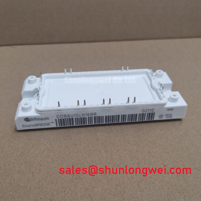
For procurement comparison, the DDB6U100N14R can be reviewed alongside the DD104N16 as a separate candidate. Treat its electrical configuration and installation requirements as independent checks rather than assuming interchangeability from a similar current class or product name.
| Selection checkpoint | DD104N16 | DDB6U100N14R |
|---|---|---|
| Rated reverse voltage | 1600 V | Consult Datasheet |
| Rated average forward current | 104 A under the specified datasheet conditions | Consult Datasheet |
| Package | PowerBlock Module | Consult Datasheet |
| Replacement approval | Match original circuit and assembly | Verify topology, terminals, dimensions, and thermal requirements |
During reassembly, distinguish mounting fasteners from electrical terminal fasteners and apply the corresponding manufacturer instructions. Check contact flatness and the specified thermal interface arrangement. ⚠️ Field Alert: Do not apply a torque value from another PowerBlock module merely because its fasteners appear similar.
DD104N16 Operational Boundaries: Evaluating Commutation Voltage Stress
Capture the voltage across the diode during commutation and correlate it with circuit current to locate reverse recovery stress and inductive overshoot. Use a measurement arrangement suitable for the circuit voltage and transient environment, keeping probe connections compact enough to limit measurement artifacts.
Design Consideration: Reverse recovery peak current and recovery time depend on forward current, temperature, and the imposed current transition. Recovery softness also affects the interaction with circuit inductance. Do not assign numerical recovery characteristics to the DD104N16 without matching manufacturer test conditions. Infineon’s High Power Semiconductor Solutions provides the manufacturer’s power semiconductor reference context.
Reduce unnecessary commutation loop area to limit inductive voltage stress, then verify the measured peaks against the device rating throughout the intended operating conditions. Inspect terminal insulation surfaces for contamination and preserve the equipment’s required clearances when routing replacement conductors.
If adjacent controlled switches influence commutation, the Precision Gate Drive Design guide provides context for assessing their drive behavior. Gate dead time, desaturation detection, and soft shutdown belong to those controlled switches. Resolve their interaction with the diode through correlated switching measurements before returning the assembly to service.