


Content last revised on September 30, 2026
Assembly Integrity and Layout Architecture for DD260N18KHPSA1
| Manufacturer | Infineon |
| Part Number | DD260N18KHPSA1 |
| Product Category | Diode Module |
| Package | PowerBlock Module |
| Working Voltage | Standard Industrial Rating |
| Rated Current | Standard Operating Current |
Isolate the DC link, discharge the capacitor bank, and measure the module terminals for an unexpected low impedance before removing the failed unit from an SVC or thyristor switched capacitor assembly. Inspect the PowerBlock housing, terminal surfaces, mounting base, and busbar contact areas for cracking, contamination, looseness, or evidence of local overheating.
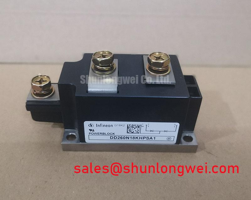
The DD260N18KHPSA1 is an Infineon diode module with a PowerBlock Module package. The supplied product data identifies its working voltage as a Standard Industrial Rating and its rated current as a Standard Operating Current; the exact voltage, current, surge current, thermal resistance, and fuse coordination values must come from the applicable manufacturer documentation for the specific production variant.
For an AC input protection network, primary spark gaps, MOVs, semiconductor fuses, and RC suppression should be coordinated as a complete system. An IEEE 61000-4-5 test level cannot be treated as the module’s standalone withstand rating. The system engineer should compare the surge waveform, prospective fault current, fuse I2t characteristic, and diode junction limits before approving the protection stage.
Keep the high-current path compact and symmetrical where the circuit topology permits. Busbar alignment, contact pressure, creepage, clearance, and the thermal interface all affect the result seen by the diode junction. Use the original mechanical hardware or a verified equivalent, and apply the fastening method specified for the assembly rather than assigning an unverified torque value to this model.
⚠️ Field Alert: Do not insert or remove the module, busbar, or sensing cable until the equipment is isolated, locked out, and verified de-energized.
Preventing Spurious Faults from Harmonic Current Injection
Capture the line current and capacitor switching waveform with an isolated measurement setup while checking whether the abnormal current appears during firing transitions, capacitor connection, or steady-state operation. Compare the affected phase with a known-good phase before replacing the DD260N18KHPSA1.
In a grid-tied SVC, changing the thyristor firing angle changes the conduction interval and the reactive current demanded by the switched branch. The diode module can be exposed to current pulses created by the surrounding converter and filter network, but its behavior should not be inferred from the controller’s firing-angle command alone. Verify actual terminal voltage, current direction, commutation behavior, and the presence of ringing at the module terminals.
Line filters should be evaluated for impedance interaction rather than selected only by nominal current. A filter resonance can increase harmonic current or create repetitive voltage stress even when the average operating current appears acceptable. Designers should verify the filter response with the installed cable, busbar, transformer, MOV, and capacitor values, then confirm the semiconductor fuse coordination against the applicable manufacturer data.
For replacement control, the neutral reference is the original module’s electrical topology, terminal arrangement, voltage class, current class, and cooling method. The related DD200KB160 may be evaluated as a separate compatible diode module option only after engineers verify voltage, current, surge, package, terminal, and thermal requirements. It should not be treated as an automatic substitute.
Protection and Reliability During High di/dt Switching
Probe the switching node and the associated thyristor gate signal at the same event, then separate a diode conduction problem from a gate-drive problem by checking whether the abnormal waveform exists when the thyristor is not being commanded. A diode module has no gate terminal, so gate pulse rise time, back-porch current, pulse trains, and negative gate bias belong to the companion thyristor control circuit.
High di/dt current transfer can produce wiring inductance voltage, common-mode ground movement, and measurement artifacts. Minimize the power-loop area and keep gate-return and power-return paths under the system designer’s control. The final decision should be based on oscilloscope measurements of peak voltage, current sharing, commutation overlap, and thermal response during the intended operating sequence.
When a braking chopper, high-power resistor bank, or bidirectional battery converter shares a DC link with the diode assembly, review the complete thermal cycle rather than relying on average current. Repetitive pulses can produce a different junction temperature profile from continuous conduction. Use the applicable transient thermal impedance network and pulse conditions from the original technical documentation to assess peak junction temperature and recovery margin.
For industrial supplier context, engineers can compare general power semiconductor qualification information through Infineon Automotive Qualified Power Modules. That material should not be interpreted as a certification statement for this diode module or for the completed SVC equipment.
Dynamic Voltage Sharing and RC Damping
Connect a differential probe across the diode module terminals and inspect the voltage during turn-off, capacitor switching, and fault interruption; look for overshoot, ringing, or unequal voltage distribution before changing the RC network.
RC snubbers, MOVs, and series saturable reactors should be selected from measured circuit energy, switching frequency, parasitic inductance, insulation limits, and the protection coordination study. The goal is to limit unwanted dv/dt turn-on in associated controlled devices and reduce localized di/dt stress, but the values are system-determined and are not factory parameters of the DD260N18KHPSA1.
Check resistor pulse capability, capacitor impulse rating, discharge behavior, physical spacing, and heat transfer under the actual duty cycle. A snubber that reduces ringing at one operating point may increase circulating current or thermal loading at another. Confirm the result with repeated switching tests while monitoring module case temperature, terminal temperature, and the DC-link waveform.
Long-duration reliability evaluation should also account for thermal cycling, surge repetition, and enclosure conditions. The Wide Bandgap Revolution technical resource provides broader semiconductor design context, but it does not replace the DD260N18KHPSA1 specification or the system-level validation required for an SVC installation.