

Content last revised on September 10, 2026
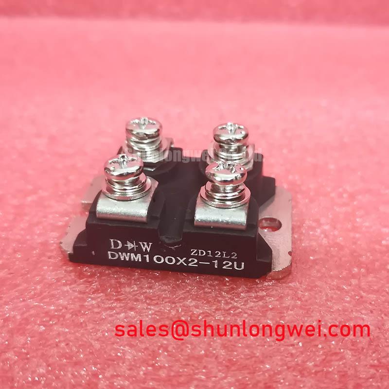
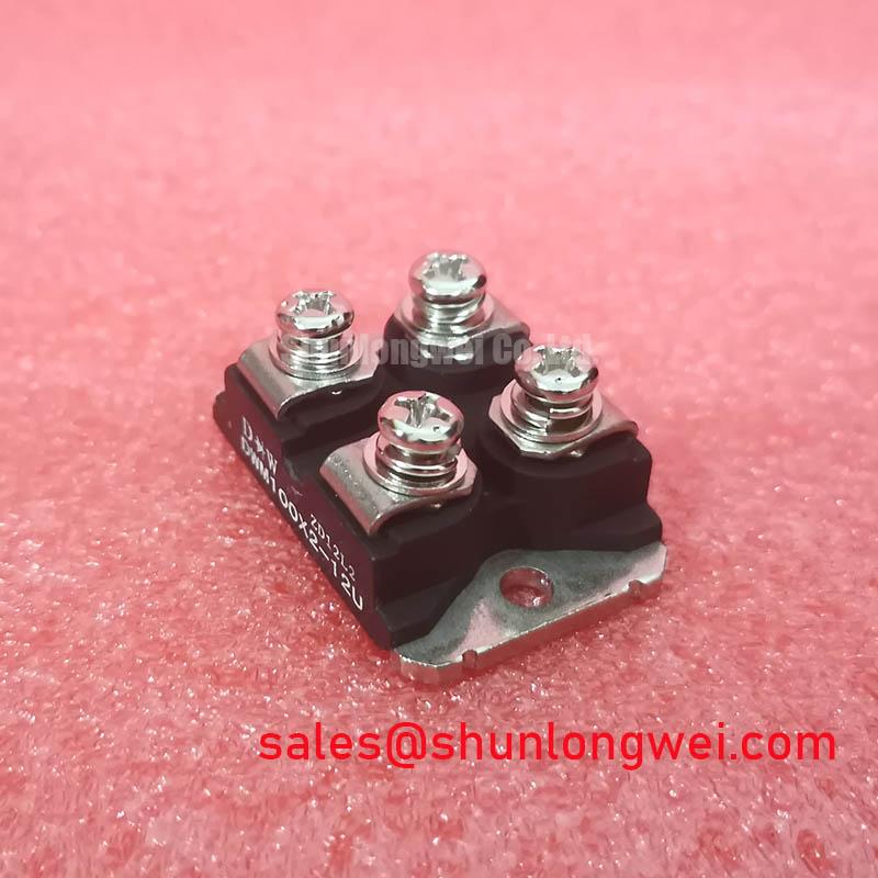
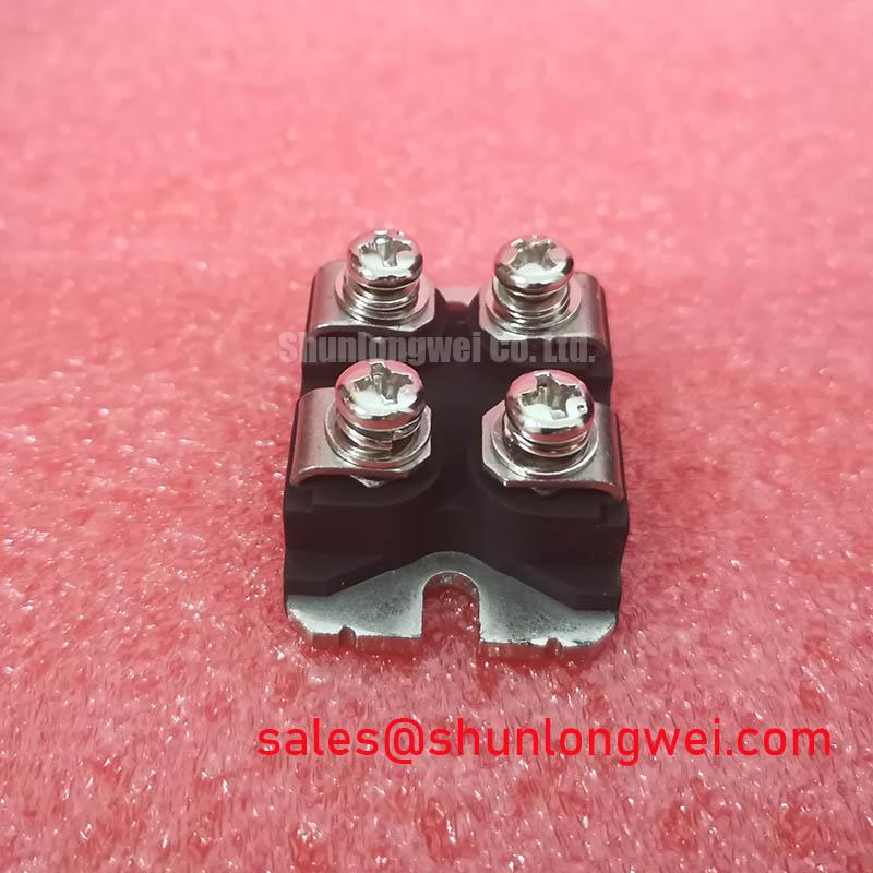
Field Diagnostics & Commissioning: Differential Gate Source Loop Routing to S in DWM100X2-12U Topologies
| Parameter | Official Specification |
|---|---|
| Manufacturer | Dawin |
| Device category | IGBT Module |
| Collector emitter voltage, VCES | 1200 V |
| Continuous DC collector current, IC | 100 A |
| Pulsed collector current, ICRM | 200 A for 1 ms |
| Maximum junction temperature, Tj(max) | 150 °C |
| Isolation test voltage, Visol | 2500 VAC for 1 minute |
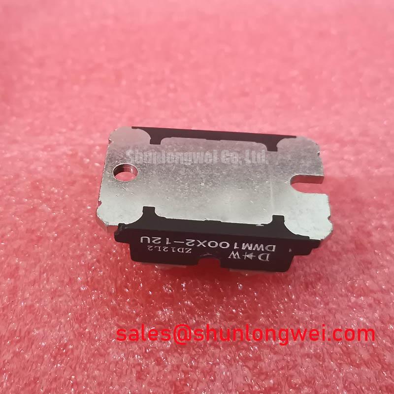
Measure the gate to source path with power removed, then compare the cold-state impedance and diode-mode response with a known-good unit from the same service population. The DWM100X2-12U is specified for 1200 V VCES and 100 A continuous DC collector current, but those ratings do not confirm the integrity of an installed gate-drive loop.
Trace the gate return separately from the main high-current emitter path wherever the physical terminal arrangement allows it. A shared copper route can introduce emitter mutual coupling during rapid current transitions, causing the measured gate-source waveform to differ from the driver reference. Use a differential probe directly across gate and source, not from gate to a distant control-ground test point. Compare turn-on delay, Miller plateau behavior, ringing, and the residual gate voltage after turn-off.
Keep the gate loop compact and route its outgoing and return conductors together to reduce magnetic loop area. Control and power conductors should not run in parallel over long distances when a switching node is nearby. If oscillation appears only at operating current, inspect the emitter return geometry, connector joints, copper overlap, and probe placement before changing the gate resistor. Designers should verify the actual clearance and creepage requirements against the system voltage, pollution environment, and applicable insulation standard.
💡 Bench Tip: Use an ESD-controlled workstation and record the cold-state gate-source measurement before connecting the module to the live converter.
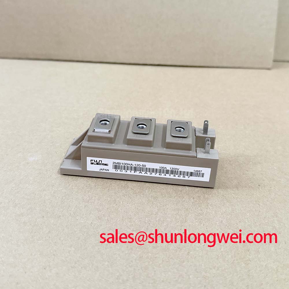
For a repair bill of materials, engineers may evaluate the electrically compatible MBM200JS12EW as a separate comparison device, subject to checking topology, mechanical fit, gate-drive conditions, and thermal requirements.
Assembly Integrity & Layout Architecture: Implementing Suppressing Cres Induced Gate Voltage Spike for DWM100X2-12U
Probe the inactive switch gate during the opposite device’s turn-on event and look for a transient gate excursion that could reduce the intended off-state margin. This check is more useful than judging the circuit from the driver supply alone because high dv/dt can couple through device capacitances and layout parasitics.
As a Design Consideration, an active Miller clamp can provide a low-impedance discharge route while the device is commanded off. Its operation must be coordinated with the isolated driver, desaturation protection, dead time, and fault reset behavior. A negative gate bias may be considered in systems where the measured off-state disturbance requires additional immunity, but the permitted gate voltage range must come from the applicable Dawin technical documentation and the complete gate-drive design.
Gate-drive sourcing and sinking capability should be selected from the required switching speed, total gate charge, driver output impedance, and acceptable transition loss. External RG damping is a Typical Starting Point for bench tuning rather than a fixed product value. Increase or decrease it only while observing gate overshoot, collector-emitter voltage, switching loss, and thermal response under the intended DC-link and load conditions.
Keep the driver return referenced to the same source point used by the power switch. Long vias, narrow neck-downs, and shared control returns can create a voltage difference that appears as unwanted gate drive. A clean hardware review should mark the gate path, source return, clamp path, isolation barrier, and switching-node boundary on the PCB drawing before commissioning.
DWM100X2-12U Circuit Protection & Reliability: Calibrating Turn-Off di/dt Induced Vpeak Clamping
Capture the collector-emitter voltage at the module terminals during turn-off and compare the overshoot with the converter DC-link voltage and the specified 1200 V VCES boundary. The inductive component of the transient rises with commutation loop inductance and current slew rate, so a high reading should trigger a layout and switching-condition review rather than a component-only diagnosis.
Use a low-inductance, symmetrical DC-link path between the commutation capacitors and the IGBT module. Plan the positive and negative bus conductors as a matched geometry, minimize unnecessary current-loop area, and keep the snubber connection physically close to the switching terminals. Snubber capacitance and damping must be calculated from measured ringing frequency, current, voltage, and acceptable loss; the final values are system-determined and require oscilloscope verification.
Check the voltage probe ground connection carefully because a long probe lead can create an artificial overshoot. Repeat the measurement with a spring-ground or suitable differential probe, then compare results at several load levels. The 200 A for 1 ms pulsed collector-current specification is an official device rating, not a blanket authorization for repetitive overload or uncontrolled surge operation. Repetitive pulse duty, junction temperature, switching frequency, and cooling conditions must be evaluated together.
Transient thermal analysis should use the applicable Zth curve and pulse profile from the device documentation when available. The specified 150 °C maximum junction temperature defines an upper boundary, while the permissible operating point depends on case temperature, mounting quality, conduction loss, switching loss, and the actual transient thermal network.
For gate-drive and commutation coordination, the engineering notes in Precision Gate Drive Design provide a relevant system-level reference. Discussions of package interconnect behavior should also distinguish verified product data from general semiconductor practice, including the principles described in Wire Bonding Metallurgical Reliability in Power Semiconductor Modules.
DWM100X2-12U Thermal-Electrical Optimization: Static and Dynamic Current Distribution Practical Tuning
Measure collector current in each parallel path and record gate-source waveforms at the same operating point before adjusting busbar or driver symmetry. The positive temperature coefficient commonly associated with IGBT saturation voltage can support static current sharing, but dynamic balance still depends on matched gate-loop impedance, commutation inductance, propagation delay, and thermal coupling.
Use symmetrical power geometry and equal-length gate-drive routes where devices operate in parallel. Inspect each source return for shared impedance, because a small transient voltage difference can alter effective gate drive during the switching edge. Engineers should verify current sharing with calibrated current probes and compare the hottest case temperature with the thermal model rather than relying on average load current.
Thermal interface preparation, clamping uniformity, heatsink flatness, and airflow should be checked during assembly. The official 2500 VAC isolation test voltage for one minute supports an insulation verification step, but the complete assembly still requires assessment of creepage, clearance, contamination, mounting hardware, and test method. Do not treat the module’s isolation test value as an independent certification of the finished inverter.
In commercial string inverters and micro-grid energy-storage converters, designers can assess this device against the required bus voltage, switching frequency, harmonic-control strategy, overload profile, and cooling architecture. Where the converter uses phase-controlled rectification or operates near a grid-current limit, measure conduction intervals and line-current harmonics at the system terminals; the IGBT module rating alone does not establish compliance with EMC or grid-interconnection requirements. Industrial display subsystems used for monitoring may be evaluated separately through their panel documentation and interface requirements, with Truly Semiconductors industrial display modules serving as an industry reference for display hardware rather than a specification for this power module.
During final commissioning, correlate electrical waveforms, case temperature, protection trips, and cooling performance over the intended load range. Any replacement or parallel-device decision should be validated for electrical ratings, gate-drive compatibility, isolation, mechanical installation, and transient behavior in the actual converter.