
Content last revised on October 27, 2026
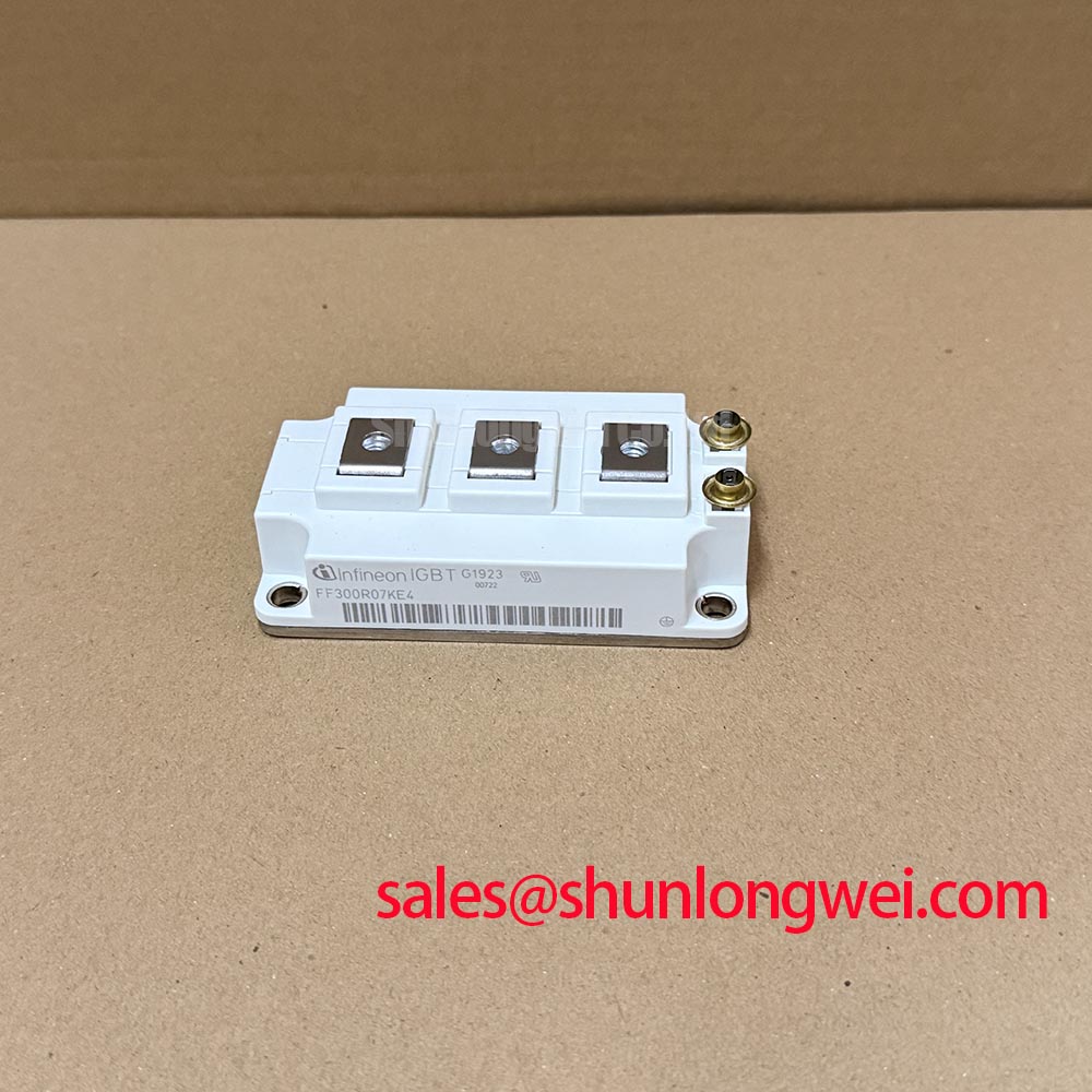
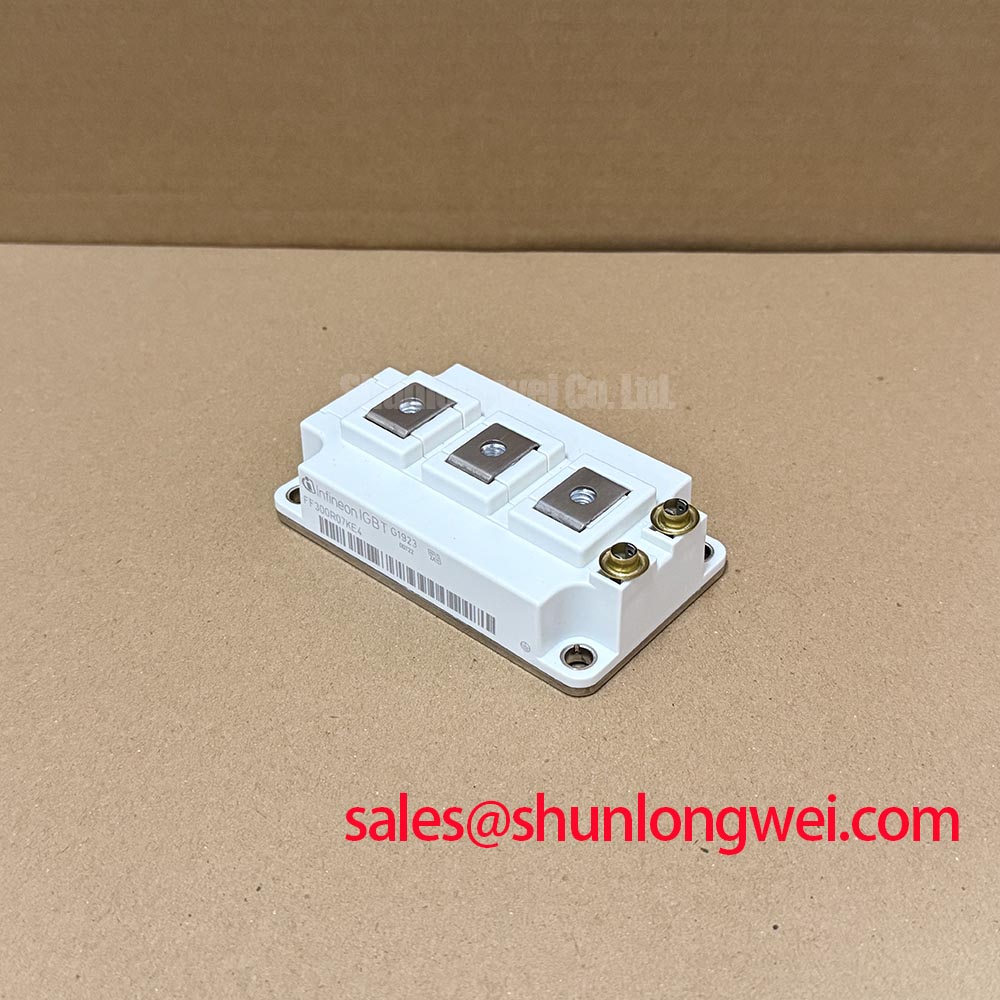
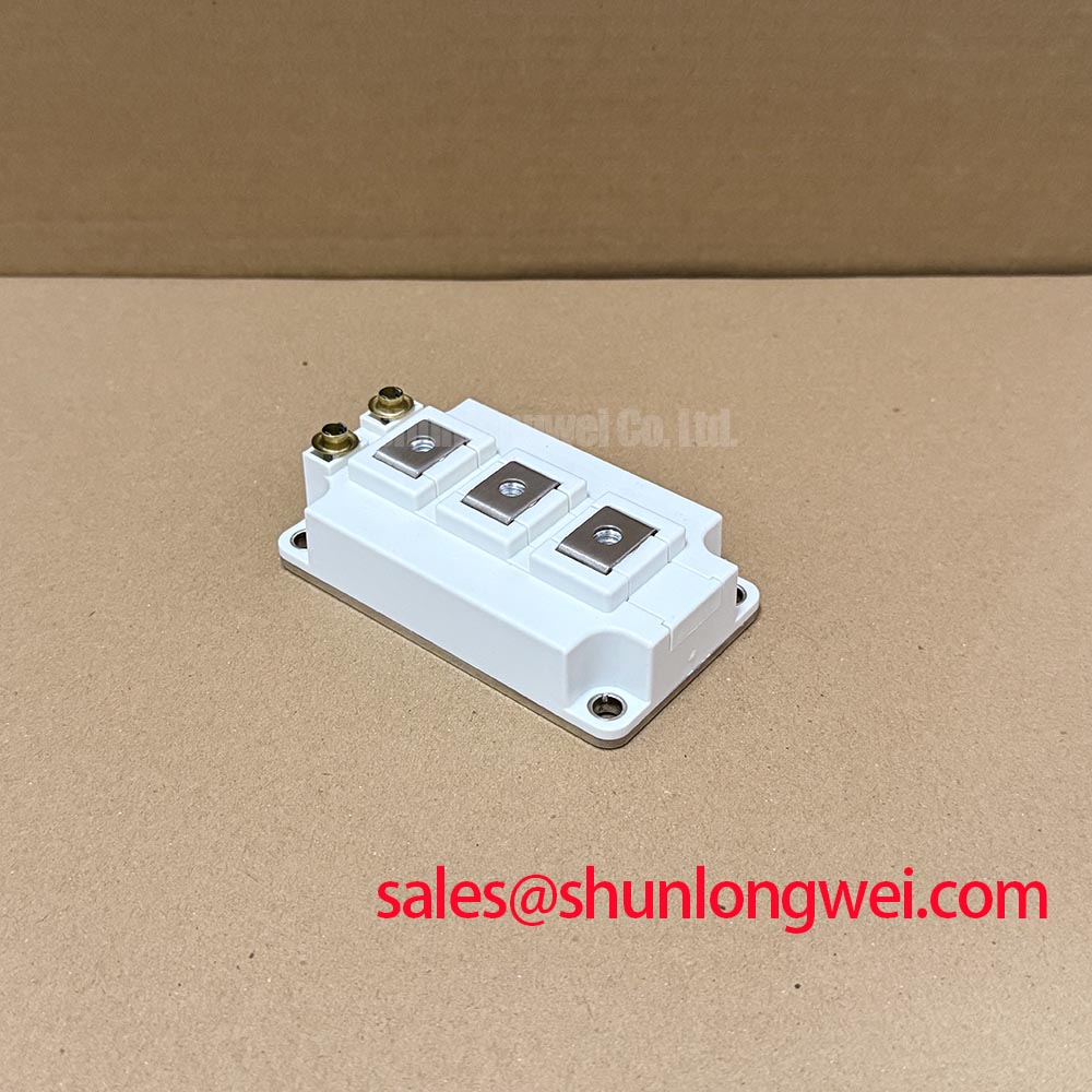
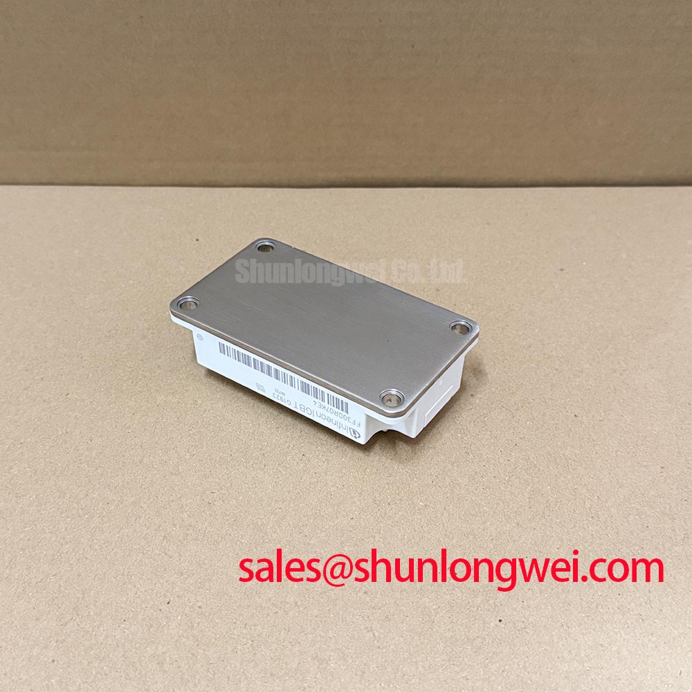
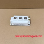
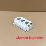
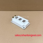
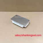
FF300R07KE4 Infineon 700V 300A IGBT Module
The FF300R07KE4 is an Infineon IGBT module with a specified voltage rating of 700 V and a rated collector current of 300 A under the datasheet conditions. Its module construction makes terminal arrangement, gate-loop routing, thermal coupling, and busbar geometry central to commissioning work. These ratings identify the device class; the permissible operating point in an inverter welder or medium-frequency induction heating supply remains dependent on switching conditions, cooling, pulse duration, protection settings, and the complete power-stage design.
| Parameter | Specification |
|---|---|
| Manufacturer | Infineon |
| Part number | FF300R07KE4 |
| Rated voltage | 700 V |
| Rated collector current | 300 A under the datasheet conditions |
| Package | Module |
Field Diagnostics & Commissioning: Separating Driver Return from Main Current in FF300R07KE4 Topologies
Gate-driver return current must not share an uncontrolled path with the high-current emitter connection. In a service inspection, first identify the main collector, main emitter, gate, and any auxiliary or Kelvin emitter connection from the applicable terminal drawing. A Kelvin emitter connection, when provided and confirmed by the device documentation, is intended to give the driver a cleaner voltage reference than the power-current path. It should not be treated as an interchangeable duplicate of the main emitter terminal.
With all power sources isolated and the DC link verified discharged, check for unintended continuity between gate and power terminals, then compare the gate-to-emitter behavior of each device position in the same bridge. A resistance reading alone does not prove semiconductor condition, but a clear imbalance between comparable device positions can justify disconnecting the driver board and repeating the test at the module interface. Keep the gate-driver return physically close to its associated gate path and avoid routing it around the power bus, snubber branch, or high-current emitter lead.
Design Consideration: Minimize the area enclosed by the gate and emitter return conductors to reduce common-emitter inductive feedback and false gate movement during rapid current transitions. The power emitter path should carry load current, while the dedicated driver return should reference the switching device as directly as the confirmed terminal arrangement permits. Clearance from adjacent collector and busbar conductors must also be assessed against the working voltage, insulation system, contamination level, and enclosure geometry rather than copied from a generic layout.
When a welder or induction-heating inverter exhibits intermittent turn-on, irregular current sharing, or unexplained gate-driver trips, compare the gate-to-emitter waveform at the module terminals rather than only at the driver output connector. Use appropriately rated isolated or differential measurement equipment. Look for ringing, displacement of the local emitter reference, and unequal timing between bridge positions. The Infineon IGBT Modules & Discretes Official Portfolio provides the manufacturer’s wider semiconductor portfolio context, while the exact terminal assignment and gate limits must be taken from the documentation for the installed variant.
For a replacement assessment, compare the electrical topology, terminal geometry, gate characteristics, internal circuit arrangement, and thermal interface requirements before treating another module as a direct substitute. The FF400R33KF2 can be evaluated as a separate device option, but its voltage class, current behavior, mechanical pattern, and driver requirements must be matched against the equipment design rather than assumed from the part number.
Field Diagnostics & Commissioning: Transient Thermal Impedance in FF300R07KE4 Topologies
Heavy pulsed overloads in welding and induction-heating converters require the junction-to-case thermal response to be treated as a time-dependent problem. A steady-state case-temperature reading can appear acceptable while a short duty burst produces a much higher junction temperature. The useful field task is to align the real pulse profile with the manufacturer’s transient thermal data and then apply the appropriate multi-RC thermal representation for the device and cooling assembly.
Start by recording pulse width, repetition rate, conduction interval, switching frequency, load current, DC-link voltage, and the measured case or heatsink temperature. Calculate conduction and switching losses using the relevant device curves and the actual gate resistance, current, voltage, and temperature conditions. A transient thermal model can then represent the junction-to-case response as several time constants, allowing the engineering team to estimate the peak junction excursion instead of relying on an averaged heat figure.
Phase-angle conduction control changes both electrical loss and thermal accumulation. If conduction is concentrated into portions of a line cycle or intermediate-frequency envelope, the thermal waveform may contain a pronounced ripple even when the external heatsink temperature changes slowly. DC-link capacitance, rectifier behavior, and load modulation should be reviewed together because ripple current can raise semiconductor loss without producing an immediately obvious change in cabinet temperature.
RC snubbers can reduce selected voltage transients, but their resistor loss, capacitor voltage rating, physical loop area, and discharge behavior belong to the complete switching network. Use the shortest practical commutation path and inspect the busbar arrangement for overlapping forward and return conductors. Reducing parasitic loop inductance is a design consideration for limiting turn-off overshoot; the resulting peak voltage must be verified during switching tests against the actual DC-link condition and the module’s official voltage rating.
For bidirectional DC-DC battery systems, repeated charge and discharge operation creates thermal cycling at the semiconductor, substrate, baseplate, and bolted interface. The evaluation should therefore include the complete temperature swing, dwell time, load profile, and cooling response. Avoid assigning a service-life figure from a generic power-cycling curve unless the curve matches the assembly, temperature range, current waveform, and mounting construction. The Precision Gate Drive Design reference can support the gate-loop and switching-test review, while the thermal calculation remains specific to the installed power stage.
Field Diagnostics & Commissioning: Preventing Terminal Overheating via Periodic Inspection in FF300R07KE4 Topologies
Terminal heating is often a joint-quality problem before it becomes a semiconductor problem. For a high-current module, use a calibrated micro-ohmmeter with a four-wire connection to examine the bolted joint, busbar interface, and cable or laminated-bus transition after isolating all power sources and verifying discharge. A low measured value is useful only when probe placement, current level, surface condition, and mechanical loading are controlled. Any joint-resistance acceptance limit should come from the equipment or assembly specification rather than being treated as an FF300R07KE4 device rating.
Thermographic inspection should be performed after the power stage reaches a repeatable operating condition. Compare equivalent terminals, phases, and bridge positions under the same load. A localized hot area at a terminal, washer, busbar step, or cable lug can indicate current crowding, inadequate contact pressure, surface contamination, or poor alignment. A broad temperature rise across the module may instead point toward cooling resistance, excessive semiconductor loss, or insufficient thermal spreading. Treat the image as a pattern to investigate, not as a single-cause diagnosis.
The baseplate must sit flat against a clean heatsink with the approved thermal interface material applied consistently. Excess compound can increase the effective thermal path and contaminate insulation surfaces, while insufficient coverage can leave voids beneath the module. The mounting sequence should maintain even contact across the baseplate, and the final torque must follow the module hardware and equipment assembly specification. Busbars should be supported so that their weight and vibration do not load the module terminals after tightening.
⚠️ Field Alert: Never reuse a loosened high-current joint without inspecting the contact surfaces and following the specified hardware, thermal-interface, and tightening procedure.
After mechanical assembly, repeat the cold electrical inspection and compare the terminal-to-busbar temperature profile during a controlled current ramp. Check that the thermal image does not show a progressive rise at one connection while neighboring positions remain stable. In an industrial inverter welder, also inspect cable flexing and vibration near the output terminals; in a medium-frequency induction-heating supply, review the busbar path for skin-effect-related current concentration and unintended magnetic coupling.
Assembly Integrity & Layout Architecture: Implementing Driver Power Stage Start-Up Inrush Mitigation for FF300R07KE4
Driver auxiliary power must reach a valid and stable state before switching is enabled. The startup sequence should keep the IGBT gates in a defined off state, confirm undervoltage lockout interlocks, and prevent PWM release until the driver supply, isolation feedback, fault reset, and cooling permissives have been accepted by the control system.
A negative turn-off bias may be used in some IGBT driver architectures, but its value must be selected from the applicable device and driver documentation. The gate-drive designer must confirm the permitted gate-emitter voltage, isolation behavior, driver output capability, Miller management, and fault response. The negative rail should be monitored for startup delay, collapse under gate-current demand, and interaction with the driver’s UVLO threshold.
Bootstrap supplies require particular attention when the upper switch remains on for an extended interval or the switching pattern provides insufficient recharge time. The bootstrap capacitor must retain sufficient charge for the complete high-side gate-drive event, including driver quiescent current, gate-charge demand, leakage, and temperature variation. The charging diode’s reverse-recovery behavior can inject unwanted current into the driver loop when the switching node moves quickly. Designers should select the charging network from the actual duty cycle and switching waveform, then verify the capacitor voltage and gate waveform at the module terminals during startup and load transitions.
Inrush mitigation belongs to the DC-link assembly as well as the control sequence. Precharge contactors, resistive charging paths, discharge circuits, and auxiliary supply interlocks should be checked for correct order and fault handling. The inverter should not release gate pulses merely because the DC-link measurement has crossed a software threshold; the driver’s local UVLO, isolation feedback, and hardware fault chain also need to be valid. During commissioning, use a controlled current-limited source where practical, then inspect gate stability before exposing the module to the full stored-energy system.
Short-circuit protection should be coordinated with the driver’s desaturation or VCE monitoring function when that architecture is used. A soft turn-off sequence can reduce the voltage overshoot associated with abruptly interrupting fault current, but its resistor, blanking interval, clamp behavior, and gate-current path are system-specific. The protection circuit must be tested with the actual bus inductance, gate loop, driver isolation, and fault injection method. Verify that the fault latch inhibits further pulses and that the reset sequence cannot restart the bridge while the cause of the trip remains present.
Before returning an industrial inverter welder or medium-frequency induction-heating supply to service, confirm the gate waveform, auxiliary supply sequencing, terminal temperature trend, and DC-link precharge behavior as one coordinated commissioning record. The FF300R07KE4 remains identified by its 700 V voltage rating and 300 A collector-current rating under the datasheet conditions; reliable field operation depends on how the surrounding power, thermal, mechanical, and protection systems are implemented and verified.