

Content last revised on October 27, 2026
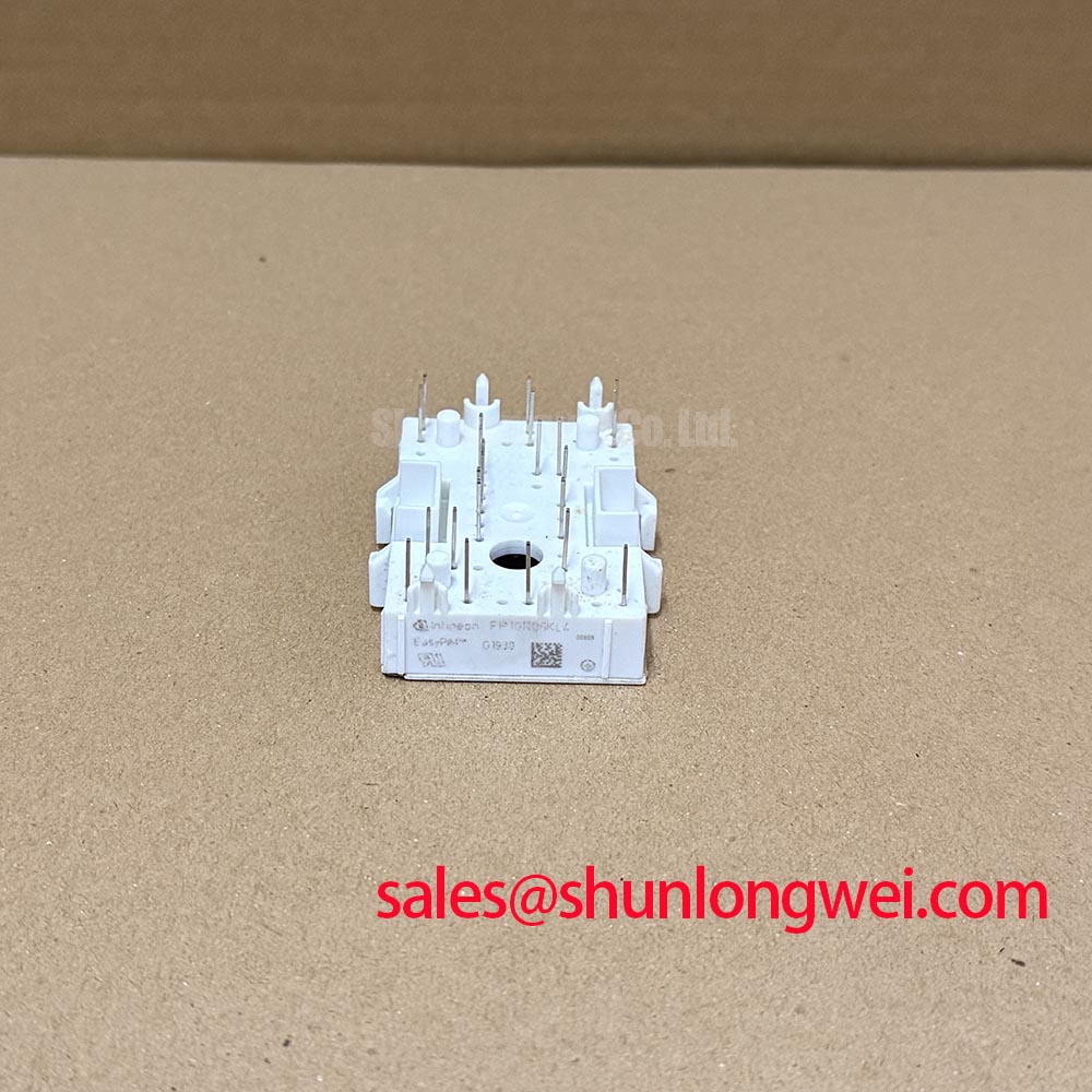
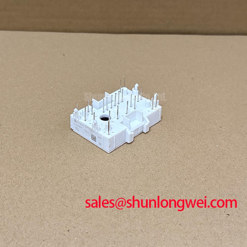
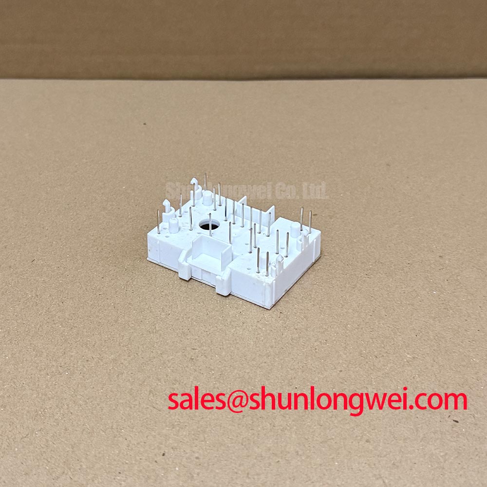
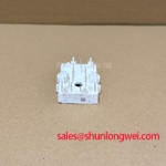
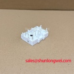
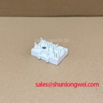
FP10R06KL4 Infineon 600V 10A IGBT Module
With the DC link isolated, discharged, and verified de-energized, check the replacement module’s terminal polarity and compare cold-state diode readings with a known-good unit before reconnecting the gate-drive board. The Infineon FP10R06KL4 is a 600 V, 10 A IGBT module; these ratings are subject to the conditions and limits in the applicable datasheet.
For a retrofit in a high-dynamics multi-axis CNC or robotics servo, the first practical question is not only whether the voltage and current labels match. The gate-drive loop, commutation path, thermal interface, and mechanical mounting surface must also remain compatible with the original topology. A replacement that fits the power stage can still produce excessive ringing if the external gate resistance or emitter return path changes.
At the incoming inspection bench, keep the device protected against electrostatic discharge and use the multimeter diode function only on an isolated, unenergized module. Record the forward conduction direction of each accessible antiparallel diode path according to the manufacturer’s terminal drawing, then compare readings between corresponding devices. A diode reading is a screening measurement, not a complete switching test; abnormal asymmetry, open conduction, or unexpected bidirectional conduction should lead to pinout verification and further de-energized checks before any controlled powered testing.
Field Diagnostics and Commissioning: Gate Drive Resistance Calibration in FP10R06KL4 Topologies
External turn-on and turn-off gate resistors determine how quickly the driver charges and discharges the IGBT gate, so a legacy servo board should be commissioned with the original gate network documented before any resistor is changed. Record the installed resistor arrangement, driver output stage, gate return path, and local bypass placement. When the FP10R06KL4 is fitted into a different switching environment, the same resistor value may not produce the same gate waveform because driver impedance, trace inductance, gate charge behavior, and collector current are system-dependent.
A practical calibration sequence starts at reduced electrical stress. Observe the gate to emitter waveform at the module terminals rather than at the driver IC, using a differential or isolated probe rated for the measurement voltage and common-mode transients, and separately monitor the collector-emitter transition with a properly rated differential probe. Never connect an earth-referenced oscilloscope ground lead to a floating emitter or switching node. The target is a clean transition with acceptable overshoot and ringing while keeping switching loss within the thermal budget established for the drive. If turn-on ringing appears, the engineer can evaluate whether the external turn-on resistance, gate loop routing, or probe connection is contributing. If turn-off overshoot is present, inspect the commutation loop and the turn-off path before simply increasing resistance.
Dead-time is equally important in a complementary bridge. It must prevent direct conduction between opposing switches while preserving the required output voltage and current response. A gate signal that appears correct at the controller can still suffer from propagation mismatch, ground movement, or Miller-related disturbance at the module terminals. During commissioning, verify both command channels, their actual gate waveforms, and the collector-emitter voltage under the intended load profile. The final dead-time value is determined by the complete driver and power-stage response, not by the module current label alone.
For high-dynamics CNC axes and robot servo inverters, the control loop may demand rapid current reversal. That makes parasitic inductance and di/dt ringing more visible than in a low-frequency test. Keep the high-current commutation loop compact, separate gate wiring from switching nodes, and provide clearance appropriate to the maximum working voltage, expected transients, and applicable insulation requirements. If a snubber is used, select and validate it from measured transient energy and switching behavior; an RC network should not be treated as a universal substitute for a low-inductance layout.
Phase-controlled front ends and thyristor-based auxiliary supplies can also affect the inverter bus. The thyristor gate trigger should be evaluated by its required gate trigger current and voltage, pulse width, and pulse-train behavior from the relevant device documentation. Conducting angle control changes line-current distortion and ripple reaching the DC link, so commissioning should include bus ripple observation and harmonic assessment where the rectifier is part of the same equipment. These are system-level conditions rather than additional ratings of the FP10R06KL4.
💡 Bench Tip: Never insert or remove the module, gate cable, or oscilloscope ground connection while the DC link or gate-drive supply is energized. Isolate all supplies, discharge stored energy, and verify the absence of voltage before making connections.
Field Diagnostics and Commissioning: Thermal Interface Material Thickness Uniformity in FP10R06KL4 Topologies
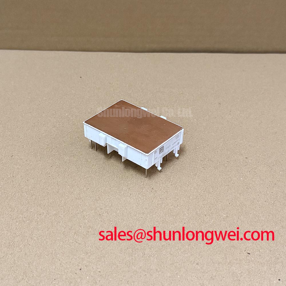
Thermal transfer begins with the contact between the module mounting surface and heatsink, so inspect flatness, surface contamination, mounting-hole alignment, and the spread of the thermal interface material before tightening the assembly. A controlled TIM layer in the 50 to 100 µm range is a general engineering starting consideration for a suitably prepared interface, not an Infineon factory specification for this part. The selected material and final thickness should follow the applicable module mounting instructions and heatsink and interface-material supplier requirements.
Apply the compound evenly enough to fill surface irregularities without creating avoidable voids. Excess material can increase mechanical compliance and contaminate nearby insulation surfaces, while insufficient coverage can leave localized dry regions. A witness inspection after a trial assembly can reveal whether the module is contacting uniformly. If the module mounting surface or heatsink shows curvature outside the permitted tolerances, correct the mechanical interface rather than attempting to compensate with an uncontrolled layer of compound.
Tighten mounting screws progressively in the sequence specified by the module mounting instructions so that the module seats evenly. Use the fastening torque specified by the module and heatsink assembly documentation. Do not substitute a remembered torque value from another package, because screw size, washer arrangement, module construction, and heatsink material can change the allowable load. After mounting, confirm that the power terminals remain aligned and that the clamping operation has not displaced the module.
| Evaluation point | FP10R06KL4 | FP100R12KT4 B11 |
|---|---|---|
| Manufacturer | Infineon | Infineon |
| Voltage rating | 600 V; subject to datasheet limits | Consult the applicable product datasheet |
| Current rating | 10 A under the specified datasheet conditions | Consult the applicable product datasheet |
| Package classification | Module | Consult the applicable product datasheet |
The comparison is a screening aid, not a substitute for checking electrical topology, terminal assignment, gate-drive requirements, thermal resistance, and mechanical dimensions. Engineers assessing a higher-voltage or higher-current alternative can review FP100R12KT4-B11, then confirm whether its ratings and interface match the servo inverter. This does not establish it as a drop-in replacement. Infineon’s IGBT Modules and Discretes Official Portfolio provides the manufacturer’s broader product context for this comparison.
Thermal commissioning should continue under the real switching pattern rather than a static current check alone. Measure case or heatsink temperature at representative acceleration, braking, and holding conditions, while observing whether line-frequency ripple or phase-angle rectifier operation changes the thermal waveform. If the front end produces a pulsating bus, evaluate the DC-link capacitor, rectifier control, and ripple current together. An RC snubber may reduce a measured switching transient, but its losses and effect on the switching waveform must be included in the thermal review.
Transient Dynamics and Electrical Design: Kelvin Emitter Connection on FP10R06KL4
Do not assume that a module described only by its package classification includes a separate Kelvin emitter terminal. First identify every power and auxiliary terminal from the correct terminal drawing for the exact device. If the installed topology provides an auxiliary emitter return, route that return directly to the gate driver reference and keep it separate from the high-current emitter path until the intended reference point.
The reason is shared inductance. When the load current changes rapidly, voltage developed across the main emitter path can move the apparent emitter potential seen by the driver. The gate loop then receives a transient reference shift that may appear as unwanted gate oscillation, delayed turn-off, or an apparent mismatch between the two bridge legs. Separating the auxiliary return reduces shared-impedance coupling when the layout permits it, but it does not remove the need to verify the actual terminal definition and driver isolation arrangement.
Keep gate and auxiliary-emitter conductors close together as a controlled loop, while keeping that loop away from the collector switching node and high-current busbars. Avoid routing the driver reference through a connector pin or copper region shared with pulsed load current. At the module, probe gate to emitter with a suitably rated differential or isolated probe and a short, low-inductance connection. Long probe leads can create ringing that is not present in the circuit and can misdirect resistor selection.
If the gate waveform changes when the load current rises, compare the local gate-to-emitter measurement with the driver-side signal. Inspect connector contact resistance, auxiliary return continuity, isolation barrier behavior, and the physical separation of the power and control paths. Oscillation can also originate from excessive loop inductance, unsuitable driver damping, insufficient local decoupling, or an interaction with the bridge commutation pattern. Each change should be tested independently so that the measured effect remains identifiable.
For equipment-level context on how IGBT switching behavior interacts with renewable-energy converters, electric-drive systems, and heavy industrial power stages, see the Industrial Applications reference. When the FP10R06KL4 is evaluated for a CNC operator system, robotics servo cabinet, or related industrial drive, the final acceptance check should cover gate waveform integrity, transient voltage margin, thermal behavior, insulation coordination, and the mechanical interface under the actual duty cycle.