Content last revised on October 13, 2026
Preventing Spurious Faults: Auxiliary Emitter Pinout Cold-Check Guidelines for FP100R12KT4-B11
With the DC link discharged and the module isolated from external current paths, match each terminal marking on the FP100R12KT4-B11 to the equipment schematic before placing meter probes across the power terminals. A reading taken through connected busbars, driver circuitry, or discharge components can describe the surrounding assembly rather than the device being checked.
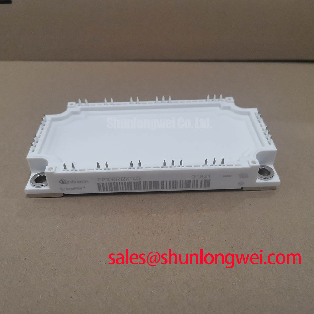
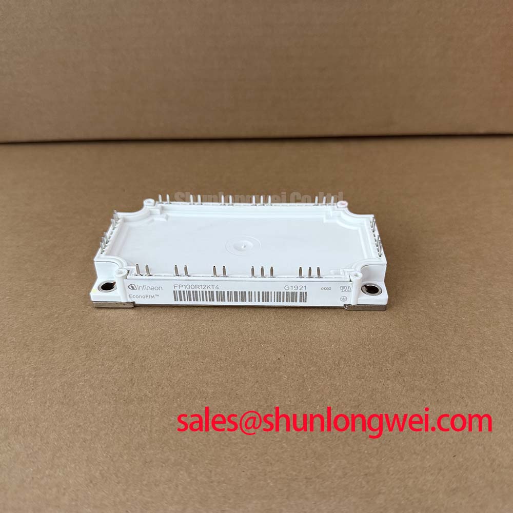
The Infineon FP100R12KT4-B11 is an IGBT Module with a rated voltage of 1200 V and rated collector current of 100 A under the datasheet-specified conditions. Its package designation is Module. For incoming inspection and replacement assessment, connect these electrical ratings to the actual terminal map, mounting arrangement, and driver interface; matching voltage and current alone does not establish equipment compatibility.
Trace the driver return connection to the emitter reference identified in the module terminal drawing, rather than choosing a return point because it appears electrically common with the power emitter. The first bench task is to establish which terminals carry load current and which connections the equipment uses for gate control. Consult the manufacturer terminal drawing for pin assignments, auxiliary-emitter availability, and mechanical details before assigning a Kelvin-return function to any terminal.
As a Design Consideration, a dedicated auxiliary emitter connection, where documented, provides the gate driver with a reference that avoids part of the voltage developed along the main emitter current path. Main and auxiliary connections can show continuity on a stationary meter while behaving differently during switching. Cold continuity therefore helps identify a connection, but it cannot demonstrate that the installed gate-return routing is suitable.
Follow the return conductor from the module interface back to the driver output stage. Check whether it shares a connector contact, PCB segment, or harness connection with a high-current return. Record the physical route as well as the schematic net name. A net labelled “emitter” does not reveal where load current enters that net or how much of the conductor is shared with the driver reference.
For an assembly reporting intermittent switching faults, inspect the driver-return contact and its mating connection before changing gate-drive components. Compare connection integrity between equivalent channels with the equipment unpowered. Contact movement, inconsistent seating, or an unintended return path can justify further investigation, but none independently proves the cause of a fault. Keep the findings tied to the measured channel and assembly condition.
💡 Bench Tip: Use ESD-controlled handling and compare cold readings with a known-good module under the same meter settings, probe polarity, and temperature conditions.
When powered testing becomes appropriate, the engineering team should measure gate-to-emitter voltage at the module interface using a suitably rated measurement arrangement. As a Engineering Recommendation, compare that waveform with the driver-side signal to locate reference movement or connection-related ringing. Use the equipment’s insulation and spacing requirements when reviewing conductor separation; an arbitrary clearance rule does not establish suitability for this module installation.
FP100R12KT4-B11 Operational Boundaries: Evaluating Cold-State Main Terminal Impedance Limits
Set the digital multimeter to diode-check mode and record both probe orientations across each power-terminal pair identified by the circuit diagram. Keep the gate in a defined off-state using the approved bench procedure. An uncontrolled gate charge can alter the apparent collector-to-emitter behavior and make repeated measurements difficult to interpret.
As a Design Consideration, the antiparallel diode associated with an IGBT switching position should be evaluated in the direction shown by the circuit symbol. Compare corresponding switching positions rather than applying a universal forward-voltage pass band. Meter test current, device temperature, and connected circuitry influence the displayed value. A diode-mode reading is a screening observation, not a measurement of the diode’s forward voltage under operating load.
A low reading in both directions, an unexpected conductive path, or a substantial difference between equivalent positions warrants isolation and repeat testing. Remove external paths that could affect the result, verify probe contact, and repeat the measurement with unchanged instrument settings. This sequence distinguishes a reproducible module-level observation from a reading caused by the surrounding assembly without assigning a single cause to the symptom.
Gate checks require a separate interpretation. A meter can reveal gross gate-to-emitter or gate-to-collector conduction, but it cannot establish compliance with a specified gate-leakage limit unless the test voltage, instrument sensitivity, and measurement method match the applicable specification. Use a controlled semiconductor test arrangement for acceptance measurements, and avoid applying an insulation tester indiscriminately across gate terminals.
The 1200 V rating describes the specified semiconductor voltage boundary; it is not an insulation-test instruction between terminals and the mounting surface. Insulation verification requires the manufacturer’s stated test configuration and the equipment acceptance procedure. On the bench record, distinguish semiconductor blocking checks from insulation checks so that a successful diode screen is not mistaken for evidence of insulation withstand capability.
For parallel operation, cold readings also cannot establish current sharing. Infineon’s IGBT paralleling application note explains why device characteristics, electrical connections, and thermal conditions must be considered together. As a Design Consideration, a positive temperature coefficient of collector-emitter saturation voltage can support static sharing in the applicable operating region, but the relevant characteristic curves must establish that region. Symmetrical busbar paths and comparable cooling remain important; a favorable temperature coefficient does not correct unequal connection impedance.
For procurement comparison, FP75R12KT3 is a separate model to evaluate against the equipment requirements, not an automatic substitute for FP100R12KT4-B11. Compare circuit configuration, current capability, terminal assignments, switching characteristics, and mounting geometry before considering a substitution. Preserve the complete model suffix in the purchasing record so that an apparently similar family designation does not conceal a relevant interface difference.
Preventing Spurious Faults: Torque Reaction Absorption Guidelines for FP100R12KT4-B11
Check fastener engagement and busbar alignment before tightening a power connection; a bolt that bottoms in its receiving thread can feel tight without producing the intended contact pressure. Where the documented terminal arrangement uses screw connections, compare the installed fastener length and washer stack with the approved assembly drawing. Use the specified hardware rather than compensating for a poor fit with additional tightening.
As a Design Consideration, the busbar should meet the terminal contact surface without using the module terminal as a lever or alignment fixture. With the connection unsecured, inspect whether the busbar naturally rests in position or must be pulled sideways to reach the hole. A forced fit transfers assembly load into the terminal interface and can complicate later assessment of connection stability.
Support the external conductor so that tightening reaction and conductor weight are controlled by the assembly, not by unsupported module terminals. Check the tool approach as well: an angled driver can introduce side loading while obscuring whether the fastener is seating correctly. Apply the manufacturer’s connection-specific torque and mounting sequence with calibrated tooling; terminal fastening and module-to-heatsink fastening should not be treated as interchangeable operations.
Washer selection and orientation belong to the documented joint design. Do not infer that a spring washer, locking feature, or increased preload is appropriate simply because the equipment experiences vibration. As a Engineering Recommendation, evaluate the contact stack, conductor support, and permitted movement together. The objective is stable electrical contact without imposing avoidable mechanical load on the module interface.
For a connection associated with intermittent faults, document seating marks, displaced hardware, and changes in contact condition before disturbing the joint. Compare equivalent connections using the same inspection method. If contact resistance is investigated, use a suitable measurement technique and account for parallel paths; ordinary probe resistance can obscure small differences. A local temperature rise should prompt investigation of current distribution and contact condition rather than an immediate diagnosis of module damage.
Mounting also affects the thermal conditions under which the 100 A rating is assessed. Inspect the heatsink mating surface and follow the approved thermal-interface application and fastening procedure. Do not introduce press-pack pressure calibration, disc-spring settings, or double-sided clamping practices without documentation identifying them as part of this assembly. The external package and mounting instructions—not a generic power-semiconductor installation habit—determine the appropriate method.
FP100R12KT4-B11 Operational Boundaries: Evaluating PCB Gate Loop Layout Symmetry Limits
Compare each gate-drive route with its corresponding emitter-return route, paying particular attention to shared conductors near the module connector. As a Design Consideration, the outgoing gate path and its return should form a compact control loop while remaining distinct from the main load-current path. Equal-looking traces are not necessarily electrically symmetrical if their return connections or nearby power conductors differ.
Where the terminal documentation provides an auxiliary emitter connection, route the driver reference through that documented interface rather than through a convenient power-return node. Check the complete loop, including connector transitions and driver-board routing. Separating the routes on one PCB section does not remove shared impedance introduced elsewhere in the assembly.
Reduce avoidable coupling between the power commutation path and the gate loop to limit induced disturbances during switching. The required layout depends on the busbar arrangement, driver characteristics, and operating conditions. Engineers should validate changes by observing gate-to-emitter behavior at the module and collector-emitter transients under controlled conditions, rather than selecting an unsupported universal trace length or inductance target.
If oscillation or unexpected protection activity occurs, compare affected and unaffected channels for return routing, gate-component placement, connector integrity, and measurement setup. Probe placement can change the observed ringing, so establish a repeatable measurement reference before modifying the circuit. The IGBT Design & Integration resource provides supporting discussion of gate-drive, thermal, and topology interactions without replacing the module-specific terminal drawing.
For commercial string inverter or micro-grid energy-storage replacement assessment, engineers should verify the original power-stage configuration, driver interface, cooling arrangement, and protection behavior against FP100R12KT4-B11. Infineon’s IGBT Modules Overview provides manufacturer context for module selection; the actual equipment interface remains the basis for compatibility.
Finally, review any desaturation-monitoring connection against the same local emitter reference used by the driver. As a Engineering Recommendation, evaluate sensing disturbances and controlled turn-off behavior together, because changing return routing can affect both gate control and fault detection. Establish protection thresholds and timing from the applicable device characteristics and system tests, then retain waveform evidence showing that the revised layout resolves the observed disturbance without introducing a new switching problem.