

Content last revised on November 6, 2026
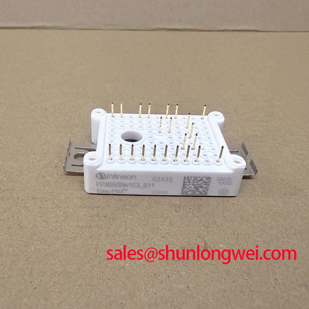
Transient Dynamics & Electrical Design: Thermal Interface Material Thickness Uniformity on FP30R06W1E3
Check the mating surface for flatness, cleanliness, and supported contact before applying thermal interface material. As a Design Consideration, interface thickness should accommodate the approved mechanical stack without creating an unnecessarily long heat transfer path. A visibly thick bead around the perimeter does not prove that the central contact area is properly filled, and a thin external edge does not establish that internal voids are absent.
Use the approved assembly drawing and interface material instructions to establish application quantity and coverage. Where a controlled dispensing or printing process is used, inspect its repeatability on representative assemblies before accepting the process for incoming repair work. Material viscosity, surface texture, assembly pressure, and the time between application and tightening can change the final distribution. The useful acceptance evidence is a repeatable contact pattern, not an assumed universal film thickness.
If contact appears uneven, inspect the heatsink and mounting arrangement before changing the compound quantity. Local contamination, burrs, distorted brackets, or unsupported mounting points can all affect seating. Curvature compensation should remain within the documented mechanical allowances; forcing the module flat with its fasteners can transfer unwanted stress into the assembly. Do not assume that a thicker interface layer is an acceptable correction for a damaged mating surface.
As an Engineering Recommendation, follow the specified fastener sequence and use calibrated tooling appropriate to the assembly instructions. Bring the mounting points into contact progressively rather than fully tightening one location while another remains unsupported. Record the hardware condition and final assembly method so that a later thermal investigation can distinguish mounting variation from electrical loading. Generic screw torque values should not replace package specific installation instructions.
Keep thermal material away from terminal contact areas and preserve the clearances established by the equipment design. Excess material near electrical connections complicates inspection and can conceal contamination. After assembly, inspect access to gate connections and ensure that mechanical loading from the control board or external wiring does not disturb module seating.
For troubleshooting, compare temperature behavior under matched electrical load, coolant or airflow conditions, and sensor placement. A warmer external reading may reflect interface resistance, higher switching loss, unequal current, or a measurement difference; it does not identify one cause by itself. Correlate the temperature trend with electrical measurements before removing the module. Where operation involves repeated heating and cooling, maintaining consistent contact and avoiding unnecessary temperature excursions are reasonable design considerations, not a quantified service life guarantee.
FP30R06W1E3 Operational Boundaries: Evaluating High-Speed Fault Management and VCE Desaturation Limits
Trace the desaturation sensing path from the power terminal connection to the gate driver fault output before assessing protection timing. As a Design Consideration, the protection chain must distinguish normal switching transitions from an abnormal rise in collector-emitter voltage while the device is commanded on. Blanking, sensing delay, filtering, driver propagation, and the subsequent turn-off waveform all contribute to the exposure experienced by the power stage.
A fault present when a switch turns on and a fault developing during conduction produce different starting conditions. Engineers should evaluate both against the applicable short circuit safe operating area and its stated test conditions. Neither the 600.0 V voltage rating nor the 30.0 A current rating supplies a permissible short circuit duration. Protection timing belongs to the coordinated device and driver design, rather than to an assumed universal detection window.
Where the controller supports staged or soft fault turn-off, examine the complete current decay and collector-emitter voltage waveform. Reducing gate drive abruptly can increase inductive overshoot, while excessive slowing can extend dissipation during the fault. The appropriate response depends on the commutation loop, fault current, gate circuit, and validated device boundaries. Initial investigation should use a controlled, energy limited procedure rather than deliberately applying a destructive fault to a replacement module.
Fuse coordination requires a separate check. As an Engineering Recommendation, compare the selected fuse’s total clearing behavior, available fault current, DC voltage suitability, and circuit inductance with the equipment’s documented protection requirements. Fuse I²t information alone does not establish that an IGBT survives until interruption. Semiconductor gate protection and upstream fault isolation perform different jobs, and a fast fuse should not be presented as a substitute for functioning gate driver protection.
Before powered testing, compare cold measurements across equivalent circuit paths with the same meter and lead orientation. In circuit readings can include parallel semiconductor paths, capacitors, and sensing networks. An unexpected reading should prompt isolation of the relevant circuit section and comparison with an established reference, not an immediate pass or fail judgment based on a generic forward voltage range.
💡 Bench Tip: Use ESD precautions and a consistent gate discharge procedure before comparing cold readings, and never treat a low energy meter check as proof that the assembly is safe to energize.
At the system drawing level, identify the rectification, DC link, switching, and protection functions separately. A module such as the BSM100GD120DLC can be reviewed as another power stage reference when documenting a wider equipment architecture, but it is not automatically a complementary rectifier or a matching companion for this part. Actual interconnection depends on the documented topology and terminal functions.
The article Unlocking 150 kW+ Charging Efficiency offers broader rectifier topology context when tracing upstream energy paths. Keep that system level discussion separate from the FP30R06W1E3 acceptance record: charging topology, fuse selection, and fault energy must not be inferred from this module’s headline ratings.
Transient Dynamics & Electrical Design: Reinforced Galvanic Gate Drive Isolation on FP30R06W1E3
Identify the isolation barrier in the gate driver assembly and its isolated power supply before selecting a dielectric test procedure. As a Design Consideration, the power module package, driver signal barrier, auxiliary supply transformer, and PCB spacing are distinct parts of the insulation system. The EasyPIM package designation alone does not establish reinforced isolation for the complete control path.
Review barrier classification using the driver and supply documentation together with the equipment’s working voltage, transient environment, and applicable safety requirements. Dielectric withstand voltage is a test characteristic, not a direct statement of allowable continuous working voltage. Creepage, clearance, insulation construction, and the complete assembly determine the relevant evaluation. Avoid applying a blanket high voltage test through connected control electronics; use the approved test nodes and procedure for each barrier.
Common mode transient immunity also belongs to the driver implementation. During switching evaluation, inspect gate-emitter voltage at the device reference connection while observing the associated power node transition with suitable measurement equipment. A pulse on the gate trace may come from real capacitive coupling, shared return impedance, or probe pickup. Compare probe placement and measurement configuration before attributing it to unwanted switching.
As an Engineering Recommendation, minimize shared impedance between the gate return and power current paths wherever the documented terminal arrangement permits. Keep the drive loop compact, preserve the intended isolation spacing, and check that the isolated supply return follows the circuit drawing. The relevant target is stable gate control during actual switching transitions, not an unsupported numerical immunity claim for the module.
If the host driver uses bootstrap supply circuitry, evaluate supply droop during the longest commanded on interval and recovery during the available recharge interval. Capacitor behavior, diode recovery, startup sequencing, and driver undervoltage response can affect the resulting gate waveform. These are host circuit checks, not confirmed internal features of FP30R06W1E3. Component values should follow the driver requirements and measured operating conditions.
Miller coupling deserves attention when the opposite switching node changes rapidly. Gate charge characteristics and reverse transfer capacitance influence the driver’s response, but reverse transfer capacitance is not interchangeable with Miller plateau charge. Where an active Miller clamp or collector voltage clamp is present, verify its connection, operating sequence, and interaction with fault shutdown against the actual driver design. The Infineon IGBT Modules & Discretes Official Portfolio provides the manufacturer’s product documentation entry point.
Close the isolation and drive inspection by recording barrier test results separately from switching observations. Retain the measurement locations, probe configuration, auxiliary supply behavior, and any gate disturbance observed during controlled operation. That separation lets the next technician distinguish an insulation assessment from a gate control problem without treating either result as proof of the other.