

Content last revised on September 25, 2026
FZ2400R17HE4P_B9 Key Specifications
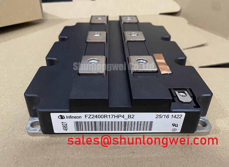
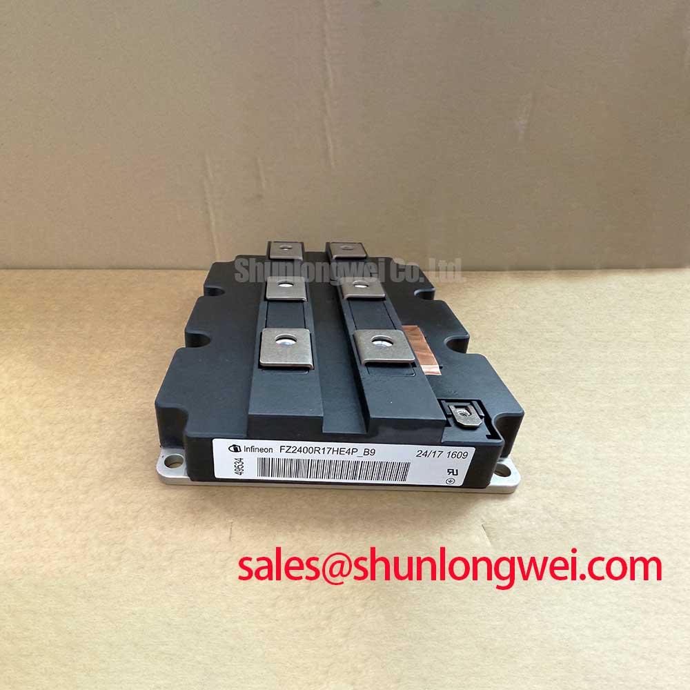
Before fitting FZ2400R17HE4P_B9, verify the cabinet nameplate, DC bus design limit, phase leg connection points, and the original drive board interface while the converter is isolated and discharged. This Infineon IGBT module is officially rated at VCES = 1700 V and IC = 2400 A at TC = 100°C. Its published operating boundary also includes Tvj op = 150°C, a typical VCE(sat) of 1.95 V at Tvj = 125°C, typical total gate charge of 23.5 mC, and a ±20 V gate emitter peak voltage. The unit uses PressFIT contacts and M8 power terminals.
| Characteristic | Official Specification |
|---|---|
| Collector emitter voltage | 1700 V |
| Continuous DC collector current | 2400 A at TC = 100°C |
| Collector emitter saturation voltage | 1.95 V typical at Tvj = 125°C |
| Gate emitter peak voltage | ±20 V |
| Total gate charge | 23.5 mC typical |
| Maximum operating junction temperature | 150°C |
| Mounting technology | PressFIT / M8 terminals |
Transient Dynamics & Electrical Design: Desaturation Detection on FZ2400R17HE4P_B9
Desaturation protection should be assessed as part of the complete gate drive and power loop, rather than as an isolated driver setting. In a high energy converter, the protection circuit monitors collector emitter behaviour after the commanded turn on interval. If a short circuit or abnormal load path causes the device voltage to remain elevated, the driver must remove the gate command in a controlled manner before the device exceeds the applicable short circuit safe operating conditions.
Type I and Type II short circuit events place different demands on the protection response. A hard short circuit can occur when a device turns on into a faulted power path. A shoot through event can occur when opposite switches in a phase leg conduct at the same time. The applicable response time, blanking arrangement, threshold behaviour, and short circuit capability must be verified against the original Infineon documentation and the actual gate driver implementation. Do not assume that a desaturation interval suitable for another IGBT family is transferable to FZ2400R17HE4P_B9.
Two stage soft turn off is a Design Consideration where inductive energy in the commutation path could create a severe collector voltage overshoot during an abrupt fault shutdown. The first stage reduces gate drive energy in a controlled way, while the final stage establishes the off state. The system engineer should capture collector emitter voltage, collector current, gate emitter voltage, and DC link behaviour during protected fault tests. This confirms that peak voltage remains inside the system validated margin against the 1700 V official device rating.
Gate loop symmetry matters at this current class. Keep the driver return path tightly associated with its gate path, minimize uncontrolled loop inductance, and keep high current power conductors away from sensitive driver sense connections. If nuisance desaturation trips occur, inspect the waveform for switching induced gate bounce, poor sensing reference placement, or noise coupling into the fault signal. Compare the affected phase with a known healthy phase before replacing protection components.
For isolated drive architectures, designers can review Infineon’s EiceDRIVER™ galvanic isolated gate driver IC information when assessing isolation strategy, common mode transient behaviour, and protection integration. Driver selection remains system dependent and must be validated at the final DC bus voltage, switching condition, and physical layout.
FZ2400R17HE4P_B9 Circuit Protection & Reliability: Calibrating Derating Guidelines and Mismatched Parameters
The typical 1.95 V VCE(sat) value is specified at Tvj = 125°C, not as a fixed field measurement target. Its positive temperature coefficient can support steady state static current sharing in appropriately paralleled IGBT arrangements, but it does not guarantee equal dynamic sharing. Differences in gate path resistance, conductor length, stray inductance, cooling contact, or driver timing can move switching energy unevenly between devices.
When evaluating parallel assemblies, verify that each device has comparable gate loop geometry and that its power path is physically balanced. Measure individual device temperatures and switching waveforms under representative load. A warmer module may reflect unequal conduction, unequal switching stress, a degraded thermal interface, restricted airflow, or a control issue elsewhere in the converter. It should not be assigned to one cause without measurement.
In utility scale centralized battery energy storage PCS equipment, phase angle control, line frequency current ripple, and bidirectional power flow are established by the converter control strategy. The IGBT module must be assessed within that strategy, including the actual modulation pattern, fault sequence, DC link arrangement, and grid interface requirements. RC snubber networks are a Design Consideration for limiting transient voltage stress where the measured switching waveform shows an inductive overshoot. Their component values, losses, and thermal ratings must be determined through system testing rather than copied from an unrelated inverter.
Protection coordination also requires attention to semiconductor fuses and the available fault energy of the DC source. Fuse I2t behaviour, contactor opening sequence, and driver shutdown timing are system characteristics. The maintenance team should verify that the actual protection chain responds predictably during approved commissioning tests and that all phase leg gate commands are inhibited after a reported fault.
For a lower current option within the same voltage class, the FF45017ME4 can be reviewed as a separate technical reference. It is not a drop in substitute for FZ2400R17HE4P_B9; current capability, mechanical interface, thermal design, gate drive conditions, and protection settings require an independent engineering comparison.
Benchtop Waveform Tuning: Mitigating Stress via High Altitude Cosmic Ray Induced SEB Failure on FZ2400R17HE4P_B9
High altitude installation can change the environmental conditions considered during converter qualification, including cooling performance, insulation coordination, and atmospheric particle exposure. No field FIT rate, single event burnout rate, altitude derating curve, or service life figure is stated here for FZ2400R17HE4P_B9. Such figures require an applicable manufacturer specification or a documented qualification source and must not be inferred from the 1700 V voltage rating alone.
For sites above 2000 m, altitude related semiconductor risk is a Design Consideration that should be reviewed by the PCS manufacturer or system engineering authority. Engineers should confirm the approved DC bus voltage range, transient peak voltage, enclosure conditions, cooling capability, and insulation design against the equipment documentation. Bench waveform measurements remain useful because they reveal whether switching overshoot, ringing, or gate disturbance changes with the installed cable arrangement and DC link configuration.
A practical waveform review starts with a correctly rated differential voltage probe and a current measurement method suitable for the expected event. Observe turn on and turn off waveforms at representative load and temperature, then compare each phase leg under equivalent conditions. A repeated voltage ring can point toward an interaction among busbar inductance, DC link capacitor placement, snubber behaviour, and gate drive speed. The corrective action should be selected only after that interaction is identified.
Long motor cables and transformer connections can introduce reflected wave effects at the system level. Their handling belongs to the output network and insulation design rather than the IGBT module alone. When FZ2400R17HE4P_B9 is installed in a battery PCS power stage, engineers should validate the converter output filter, cable route, termination conditions, and measured peak voltage using the final installation arrangement.
Where a wider power conversion chain includes a complementary high current module, the FZ3600R12HP4 may be relevant for separate topology review. Its ratings and integration conditions must be evaluated independently; it should not be treated as evidence of compatibility with the 1700 V module.
Preventing Spurious Faults: Optimizing Heatsink Contact Pressure and Service Guidelines for FZ2400R17HE4P_B9
Before mounting, inspect the heatsink surface for embedded debris, corrosion, handling damage, and uneven thermal compound residue. Confirm that the module baseplate and heatsink surfaces are clean and that the original equipment assembly method is followed. A thin, continuous thermal interface layer is a Design Consideration intended to fill microscopic surface variation without creating an unnecessarily thick thermal barrier. If a thermal interface material supplier specifies a thickness window, follow that product documentation and validate contact quality during servicing.
Baseplate flatness, mounting sequence, and torque consistency influence thermal contact across the module footprint. Tighten mounting hardware in a controlled cross pattern using the original equipment torque specification. The published module information identifies M8 terminals, but it does not provide a terminal or heatsink torque value in the stated specifications. The service technician should therefore use the converter manufacturer’s documented torque procedure rather than applying a generic value.
⚠️ Maintenance Note: Periodically monitor contact temperature rise, confirm terminal tightness during scheduled shutdowns, and keep heatsink fins and forced air paths free of dust accumulation.
Moisture control is equally important in industrial enclosures. Condensation can affect busbar insulation, gate drive boards, current sensors, and connector interfaces even when the semiconductor itself shows no obvious physical damage. Inspect cabinet seals, heater or ventilation function where fitted, drain paths, and evidence of moisture tracking. In cold start conditions, follow the equipment manufacturer’s energization procedure so that the power stage is not operated before enclosure conditions are acceptable.
If recurring overtemperature or unexplained fault reports remain after cleaning and mechanical checks, compare heatsink temperature, drive waveforms, DC link ripple, phase current balance, and airflow across operating states. The broader methods for gate drive integration, thermal management, and power circuit assessment are covered in this IGBT Design & Integration technical resource. For reverse conduction considerations in IGBT based power stages, consult Infineon’s RCDC application note alongside the applicable converter schematic and original module documentation.