Content last revised on September 13, 2026
Field Diagnostics & Commissioning: PCB Gate Loop Layout Symmetry in FS50R06KE3 Topologies
| Manufacturer | Infineon |
| Part Number | FS50R06KE3 |
| Product Category | IGBT Module |
| Rated Voltage | 600.0 V, Official Specification |
| Rated Current | 50.0 A, Official Specification |
| Package | Module, Official Specification |
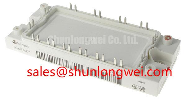
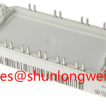
Before energizing a repaired inverter, verify the nameplate ratings, inspect the module body and terminals, and compare cold-state resistance readings with a known-good reference from the same circuit. The FS50R06KE3 is an Infineon 600.0 V, 50.0 A IGBT module in a module package, intended for evaluation in power conversion assemblies where the electrical, thermal, gate-drive, and mechanical interfaces match the original design documentation.
This product page focuses on practical integration for industrial hardware engineers and sourcing teams. The published voltage and current values above are Official Specification data supplied for this product listing. Switching frequency, short-circuit withstand capability, gate-emitter voltage limits, thermal resistance, diode characteristics, internal circuit topology, terminal arrangement, and mechanical dimensions should be confirmed against the applicable Infineon documentation before production release.
During commissioning, begin at the gate-drive connector rather than at the control firmware. With the DC link safely discharged, inspect the gate wiring, emitter return path, connector seating, solder joints, and power-loop routing. A resistance or diode-mode comparison can identify an open gate path, an unexpected short, or a difference between parallel switching positions, but a static meter reading does not prove dynamic switching integrity.
The gate loop should be treated as a high-current transient circuit. Keep the outgoing gate conductor and its return path physically close, and avoid routing the gate return through the high-current emitter path when the module provides a separate control return. The purpose of this arrangement is to reduce mutual emitter coupling and prevent voltage developed by the load-current transition from appearing as an unintended gate signal. The exact terminal assignment must be checked against the original module drawing and the drive board schematic.
Symmetry is important when multiple switching paths share a DC link. Unequal conductor length, different copper widths, or an unbalanced connector transition can cause one device position to experience a different gate waveform from another. When an inverter shows irregular current sharing, unexpected gate ringing, or intermittent protection trips, compare the gate-to-emitter waveform directly at the module terminals. The signal should be evaluated during the actual switching event with suitable probing technique, not inferred from the driver output measured several centimeters away.
A practical field sequence is to inspect the isolated gate supply, confirm the driver reference, check the turn-on and turn-off commands, and then use a controlled low-energy test before applying full operating power. If the measured waveform differs from the known-good phase, examine the local return connection, connector inductance, driver ground bounce, and clamp network. These observations may indicate a layout or signal-integrity issue, but the final diagnosis should be based on comparative oscilloscope measurements and protection-event records.
Designers evaluating this module in a robotic axis inverter or light industrial automation drive should verify the complete commutation loop, including the upper and lower switching devices, DC-link laminations, current sensors, and braking branch. Regenerative braking can return energy to the DC link, while a braking chopper and resistor absorb energy when the system control strategy requires it. The resistor rating, chopper control threshold, pulse duration, and cooling arrangement are system-level decisions and should not be inferred from the module’s 600.0 V and 50.0 A listing values alone.
For maintenance teams comparing physically related replacement options, the FS200R06KL4 can be reviewed as a separate device. Compatibility must be established from electrical ratings, internal topology, gate requirements, pin configuration, mechanical fit, thermal performance, and the original equipment documentation rather than from package appearance alone.
FS50R06KE3 Operational Boundaries: Evaluating Active Miller Clamp Implementation Limits
An active Miller clamp can help prevent an inactive switch from receiving an unintended gate voltage during the opposing device’s transition. Its effectiveness depends on the complete gate-drive impedance, the driver’s reference connection, the module terminal arrangement, the switching speed, and the common-emitter voltage movement. It is therefore a Design Consideration for the surrounding drive circuit, not an independent operating specification of the FS50R06KE3.
When evaluating cross-conduction risk, observe both gate-emitter voltage waveforms at the same time as the collector-emitter transition and phase current. A short negative-going disturbance or a positive gate excursion on the inactive channel may be associated with Miller coupling, common-emitter inductance, probe error, or an unsuitable driver return path. The oscilloscope setup should use an appropriately compact connection method and verified common-mode capability.
Negative gate turn-off bias is sometimes evaluated in high-noise bridge circuits, particularly where long gate connections, high switching transients, or large power-loop commutation events are present. The required value is system-determined. Designers should confirm the module’s permitted gate-emitter range from the applicable Infineon datasheet and ensure that the driver does not exceed that boundary during startup, shutdown, fault clearing, or isolation-power imbalance.
Phase-angle conduction control and line-frequency ripple smoothing should be assessed together. A controller that changes duty ratio or phase angle can alter the thermal pattern, current ripple, and switching-event frequency seen by the module. The 600.0 V voltage rating and 50.0 A current rating are Official Specification values, but the usable operating point depends on junction temperature, switching conditions, cooling, transient overshoot, and the converter’s protection response.
RC snubber networks may be considered when measured ringing remains excessive after the gate loop and commutation layout have been corrected. Snubber selection should be based on measured ringing frequency, energy, voltage stress, pulse repetition, capacitor dielectric behavior, and resistor temperature. It should not be selected from a generic formula without confirming the actual parasitic network. A snubber that reduces voltage ringing can also increase switching loss, so the thermal consequence must be checked under representative load conditions.
For background on the manufacturer’s power semiconductor portfolio, engineers can consult the Infineon IGBT Modules & Discretes Official Portfolio. The Infineon TRENCHSTOP™ IGBT3 application note provides additional manufacturer-published context for IGBT switching behavior; engineers should still use the device-specific documentation for final design verification.
Preventing Spurious Faults: High-Frequency Common-Mode Bearing Current Guidelines for FS50R06KE3
Long motor cables can behave as transmission-line structures rather than simple resistive loads. Reflections at the motor terminals, cable discontinuities, connector transitions, and filter interfaces can increase the voltage stress seen by the inverter output stage. The resulting common-mode current can travel through motor frames, cable shields, bearings, encoder wiring, and protective-earth paths, potentially appearing as nuisance feedback faults or unexplained electromagnetic interference.
During troubleshooting, record the DC-link voltage, phase-to-phase output waveform, phase-to-frame waveform, motor cable arrangement, shield termination, and fault timing. Compare the same measurements with a short test cable where safe and practical. A difference between the two conditions may indicate transmission-line interaction, common-mode coupling, or filter resonance. It does not by itself establish that the FS50R06KE3 is defective.
Output chokes, dv/dt filters, common-mode cores, and properly implemented motor-cable shielding can be evaluated as system-level countermeasures. Their selection depends on motor insulation requirements, cable length and construction, carrier frequency, leakage current, drive output impedance, control-loop stability, and thermal loading. Designers should verify the peak terminal voltage and common-mode current during switching tests rather than relying on a nominal DC-link calculation.
Care is also required around the freewheeling diode path. Reverse-recovery behavior influences commutation current, voltage overshoot, and radiated noise. A softer recovery characteristic may reduce one form of disturbance, but the complete bridge still has to be assessed for switching loss, dead time, current commutation, and thermal balance. These properties must be confirmed from the applicable device documentation and test data; they should not be assigned to this product listing without a source.
Gate-driver isolation and cable shielding should be treated as separate design functions. Shield current should not be allowed to share a sensitive control reference unintentionally, while the gate-drive return should follow the intended module terminal path. If a drive reports intermittent overcurrent or encoder communication faults, inspect the grounding topology, shield termination, isolated supply behavior, and oscilloscope evidence before changing protection thresholds.
The Precision Gate Drive Design technical resource can be used as a supporting reference when reviewing gate-loop impedance, return-current control, and switching-test methods. It does not replace the original equipment manufacturer’s wiring diagram or the Infineon documentation for the FS50R06KE3.
Transient Dynamics & Electrical Design: Baseplate Thermal Grease Layer Control on FS50R06KE3
Thermal installation begins with mechanical inspection. Check that the heatsink contact area is clean, flat within the equipment manufacturer’s tolerance, and free from burrs or particles. Inspect the module baseplate for contamination, visible deformation, or damage around the mounting points. A thermal interface compound should be applied as a thin, continuous layer sufficient to fill surface irregularities without creating unnecessary separation between the baseplate and heatsink.
Void control matters because trapped air increases thermal impedance and can produce local temperature differences across the module. Spread the compound according to the material supplier’s process instructions, then position the module without sliding it across the prepared surface. If the heatsink or baseplate has measurable curvature, the mechanical assembly should be reviewed before installation; excessive correction through screw force can distort the package or create uneven pressure.
Use the equipment manufacturer’s specified fastener sequence and torque procedure. A cross-pattern or staged sequence is commonly considered a Design Consideration for distributing pressure, but the correct torque remains dependent on the module construction, fastener size, washer arrangement, heatsink design, and manufacturer instructions. After tightening, inspect for baseplate rocking, extrusion of the interface compound, or movement caused by nearby busbar installation.
⚠️ Field Alert: Disconnect power and verify the DC link is discharged before touching the module terminals, gate connector, or heatsink fasteners.
Double-sided cooling, clamping hardware, and spring-loaded mounting arrangements require particular attention to pressure calibration. If a pressure indicator, disc spring, or specified tightening sequence is used by the original assembly, record its condition and compare it with the service documentation. Do not assume that a visually similar fastener provides the same mechanical load. Uneven pressure can increase thermal resistance, stress the substrate, or cause long-term changes in contact quality.
After installation, validate the thermal path under the actual load profile. Measure heatsink temperature at a repeatable location, monitor module case behavior where access permits, and compare phase temperatures during motoring and regenerative braking. Thermal imbalance can result from current sharing, switching loss, cooling airflow, interface quality, sensor placement, or control timing. The observation should be correlated with electrical waveforms rather than attributed to thermal grease alone.
Before releasing a repaired light industrial automation inverter or multi-joint robotic articulator drive, complete a staged test covering gate signals, DC-link behavior, braking energy absorption, output waveform quality, protection response, and thermal stabilization. The FS50R06KE3 identity for this listing is limited to the stated Infineon manufacturer, 600.0 V rated voltage, 50.0 A rated current, and module package. All other application limits should be verified from the controlling datasheet and system design records.