Content last revised on September 13, 2026
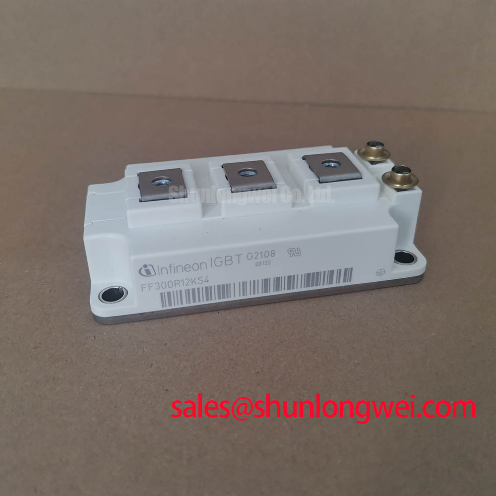
Assembly Integrity & Layout Architecture: Implementing Static and Dynamic Current Distribution for FF300R12ME4_B11
Start a field replacement with a cold inspection rather than a powered test. Look for cracked moulding, displaced terminals, contamination around the power interface, and marks that suggest excessive mechanical loading. With the module fully disconnected, compare diode and transistor paths with a known good assembly using the same meter range and probe polarity. A resistance reading is only a screening observation; it is not an official pass or fail limit for this model. If the result is abnormal, repeat the measurement after separating the module from the surrounding buswork and gate circuit.
Static current sharing in paralleled IGBT arrangements is influenced by the positive temperature coefficient of collector emitter saturation voltage. That characteristic can support balancing as devices warm, but the complete result still depends on semiconductor spread, bus resistance, emitter path symmetry, thermal coupling, and the control method. Designers should verify current sharing at the actual load point rather than infer it from the 300 A catalogue class.
Dynamic sharing is more sensitive to the physical gate loop. Keep the drive paths from the driver output to each gate electrically similar, with comparable conductor length, return path, routing environment, and connection quality. Minimize the common inductance shared by power commutation and gate control loops to reduce turn off overshoot and gate ringing. The acceptable parasitic level is system determined and should be validated with an oscilloscope using suitable high bandwidth voltage and current probes.
For an industrial inverter welder or medium frequency induction heating supply, inspect laminated busbar joints, flexible links, gate connectors, and the emitter return path as one assembly. A loose power connection can create local heating while a poor gate return can produce uneven switching that appears to be a semiconductor fault. If the original layout cannot be restored, engineers should document the new conductor geometry and repeat switching waveform checks at controlled operating conditions.
When repair logistics require evaluation of a related high power module, the FZ3600R12HP4 may be reviewed as a separate compatibility candidate. It should not be treated as an automatic substitute. Pin mapping, electrical ratings, gate characteristics, thermal interface, and mechanical fit must all be confirmed by the system designer.
⚠️ Field Alert: Disconnect the DC link and gate drive supply before inserting or removing connectors, and follow the original fastener specification with even mounting pressure and a uniform thermal interface.
FF300R12ME4_B11 Operational Boundaries: Evaluating DC Bus Operating Voltage Headroom and Derating Limits
The official voltage value for this listing is 1200.0 V. It is not a recommended DC bus operating value. During switching, the semiconductor experiences the DC link together with transient overshoot created by commutation inductance, wiring, busbar geometry, reverse recovery, and gate timing. The design team must measure the highest collector emitter voltage at the module terminals under the intended current, temperature, and switching conditions, then compare that result with the applicable manufacturer switching and safe operating limits.
Altitude deserves separate treatment. Reduced air density can affect external clearances, cooling performance, enclosure airflow, and the behaviour of insulation systems. Terrestrial neutron exposure and single event burnout are reliability subjects that require a qualified source, device technology data, mission profile, and voltage stress model. No FIT value or SEB failure rate should be assigned to FF300R12ME4_B11 from altitude alone. Engineers evaluating equipment above 2000 m should obtain the applicable manufacturer or reliability study and combine it with measured DC bus stress, environmental data, and protection response.
Switching frequency also changes the balance between conduction loss, switching loss, heat sink capacity, and transient stress. A 2 kHz to 16 kHz range cannot be treated as a universal operating envelope for this module without official loss curves and thermal conditions. The system integrator should calculate losses using the actual current waveform, gate resistance, junction temperature, modulation pattern, and switching energy data, then confirm the result through thermal measurement. Airflow requirements are enclosure specific; verify fan direction, filter condition, heat sink cleanliness, and temperature rise at the most restrictive installation point.
During a suspected overvoltage fault, capture the collector emitter waveform at the module rather than at a distant bus capacitor. Inspect the DC link capacitor connections, snubber network, busbar overlap, and commutation loop. If a protection trip occurs only at high load or high temperature, compare the event timing with gate signals and current measurement. This approach separates possible gate drive disturbance, layout inductance, thermal stress, and control protection interaction without assigning a single cause prematurely.
FF300R12ME4_B11 Operational Boundaries: Evaluating Thermal Cycling Margins of Braking-Path Limits
A braking circuit must be evaluated as an energy management system, not by the IGBT current rating alone. During motor deceleration, kinetic energy may raise the DC link until the braking path transfers energy into a braking resistor. The required braking transistor, resistor, switching controller, and protection scheme depend on motor inertia, speed profile, regeneration time, duty cycle, DC link capacitance, allowable bus voltage, and cooling conditions.
The 300.0 A official current value describes the product class supplied for this listing; it does not define a braking pulse rating, resistor power rating, overload duration, or thermal cycling limit. Designers should obtain the relevant pulsed current, switching, transient thermal impedance, and safe operating information for the exact device revision. Where the braking element is external, confirm resistor pulse energy, average dissipation, enclosure temperature, clearance, and fault containment independently of the semiconductor selection.
Transient thermal impedance is important because a short braking event may produce a junction temperature peak before the heat sink temperature changes appreciably. A thermal network assessment should use the actual pulse width and repetition pattern, then compare the predicted junction temperature with the applicable rated limits. When those curves are unavailable, the result should remain an engineering estimate rather than a product guarantee. Thermocouple readings on the case can support the investigation, but they do not directly measure the silicon junction.
In a service visit, inspect the braking resistor for surface damage, altered resistance, loose terminals, and restricted airflow. Check the DC link trend during a controlled deceleration and correlate it with the brake gate signal. A brake that activates late may involve control timing, voltage sensing, wiring, or protection logic. A brake that activates repeatedly may be correct operation under excessive regenerated energy. Review the complete deceleration profile before replacing the module.
For systems combining an input rectifier stage with an inverter and braking branch, engineers may consult the related FZ800R12KS4_B2 as a separate topology reference. It is not presented as a specified replacement for the FF300R12ME4_B11. System voltage, current path, control timing, and thermal requirements must be checked at the equipment level. Additional integration guidance is available in IGBT Design & Integration.
Preventing Spurious Faults: Negative Gate Bias and Active Miller Clamp Guidelines for FF300R12ME4_B11
A replacement module should not be connected to an unfamiliar driver until the gate supply arrangement and signal reference have been traced. The official data supplied for this listing does not specify a positive gate voltage, negative gate bias, Miller clamp threshold, gate charge, internal gate resistance, or driver output current. The system integrator should verify every one of these values from the exact manufacturer documentation and the existing gate driver design.
High dv/dt at the switching node can couple through the Miller capacitance and lift the gate of the opposite device. This can create unwanted current or a protection event, but the observed symptom may also involve common emitter inductance, driver saturation, insufficient isolation, probe connection, or timing overlap. Use a differential probe at the gate and emitter reference, observe both complementary channels, and compare the waveform with the known good phase leg. The probe return path must not introduce a new loop that changes the result.
An active Miller clamp can provide a low impedance discharge path when the controlled device is commanded off. Its usefulness depends on driver topology, clamp timing, gate loop inductance, isolation strategy, and the voltage present at the switching node. Designers should place the clamp return according to the driver manufacturer’s layout guidance and verify that it does not interfere with the intended turn on transition. The final clamp threshold and gate damping remain system determined.
Negative gate bias is sometimes used to increase immunity against false turn on, but the permitted negative gate emitter range is device specific. Do not apply a negative supply simply because another IGBT module uses one. Verify the exact maximum and minimum gate ratings, driver startup behaviour, dead time, fault reset sequence, and power supply transient response. If the driver supply collapses, an incorrectly arranged negative rail can impose a damaging gate condition even when the power stage is disabled.
Gate ringing should be checked at the module pins under real commutation current. Inspect the gate resistor connection, driver decoupling, isolated power supply, gate return conductor, and connector contact resistance. If ringing changes after the module is mechanically installed, review the routing and parasitic loop rather than changing the gate resistor blindly. Validate turn on, turn off, short circuit protection, and desaturation response together before returning the industrial welder or induction heating supply to service.