


Content last revised on September 10, 2026
Transient Dynamics & Electrical Design: DC DC Converter Interleaving and Ripple Cu on FS75R12KE3_B9
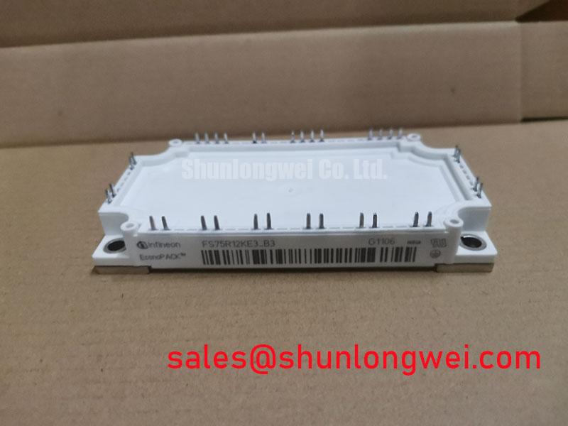
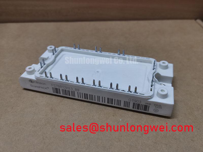
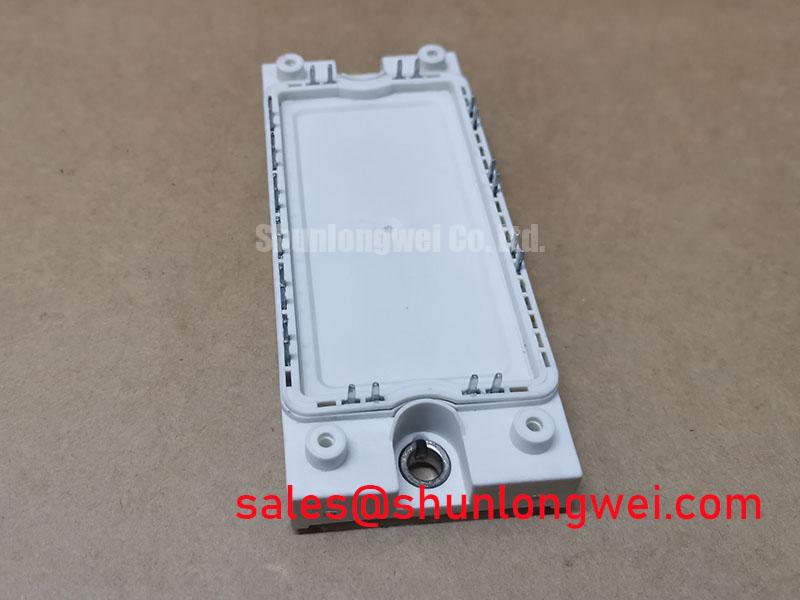
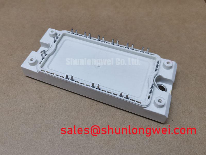
Before connecting the power circuit, verify the equipment bill of materials and the module marking against the required FS75R12KE3_B9 reference, then confirm that the converter DC link and expected load current remain within the module’s 1200 V and 75 A specified ratings and their applicable conditions. This Infineon power semiconductor is supplied as an IGBT Module; any replacement assessment must also confirm the original terminal arrangement, gate driver interface, heatsink interface, protection strategy, and control firmware compatibility.
| Parameter | Value | Status |
|---|---|---|
| Product model | FS75R12KE3_B9 | Official product identification |
| Manufacturer | Infineon | Official manufacturer identification |
| Rated voltage | 1200 V | Official specification |
| Rated current | 75 A | Official specification |
| Package category | Module | Official specification |
For a commercial string inverter or micro grid energy storage converter, the FS75R12KE3_B9 should be evaluated as part of the complete power path rather than as an isolated current switch. Battery rack charging, discharge operation, inverter DC link support, and load transients can impose changing current direction and cyclic thermal loading on the switching stage. The official device boundaries remain 1200 V and 75 A, while the actual operating stress is determined by the converter topology, switching conditions, coolant or airflow performance, fault response, and control sequence.
When an interleaved DC DC stage is involved, phase current sharing should be checked with real operating waveforms rather than inferred from controller commands alone. Differences in copper path resistance, current sensor offset, driver propagation delay, or magnetic component tolerance can shift loading between parallel paths. This may create uneven thermal cycling even when the average converter output appears balanced. A practical verification method is to capture inductor current, DC link voltage, gate command timing, and case temperature under charge and discharge transitions. The measured data should be compared against a known stable operating condition and the original system requirements.
Design Consideration: copper geometry affects both conduction distribution and switching stress. Keep high current routes direct and physically balanced where the converter uses equivalent phase branches. The outgoing and return conductors should be arranged to reduce the loop area that carries switching current. This reduces inductive voltage excursion during rapid current changes and makes waveform comparison between phases more meaningful. The applicable spacing, insulation coordination, conductor cross section, and enclosure clearance must be established by the system designer according to the installation environment and governing equipment requirements.
Ripple current in bus capacitors and laminated copper structures also needs system level review. A module replacement cannot correct a degraded capacitor bank, loose busbar interface, oxidized high current contact, or control timing error. If a converter produces elevated ripple voltage after repair, inspect the DC link capacitor condition, verify connection resistance under de energized conditions, and observe switching current with suitable isolated measurement equipment. A ringing waveform may indicate several interacting variables, including layout inductance, capacitor placement, driver behavior, or probe technique. It should be investigated against the known good signal path before changing component values.
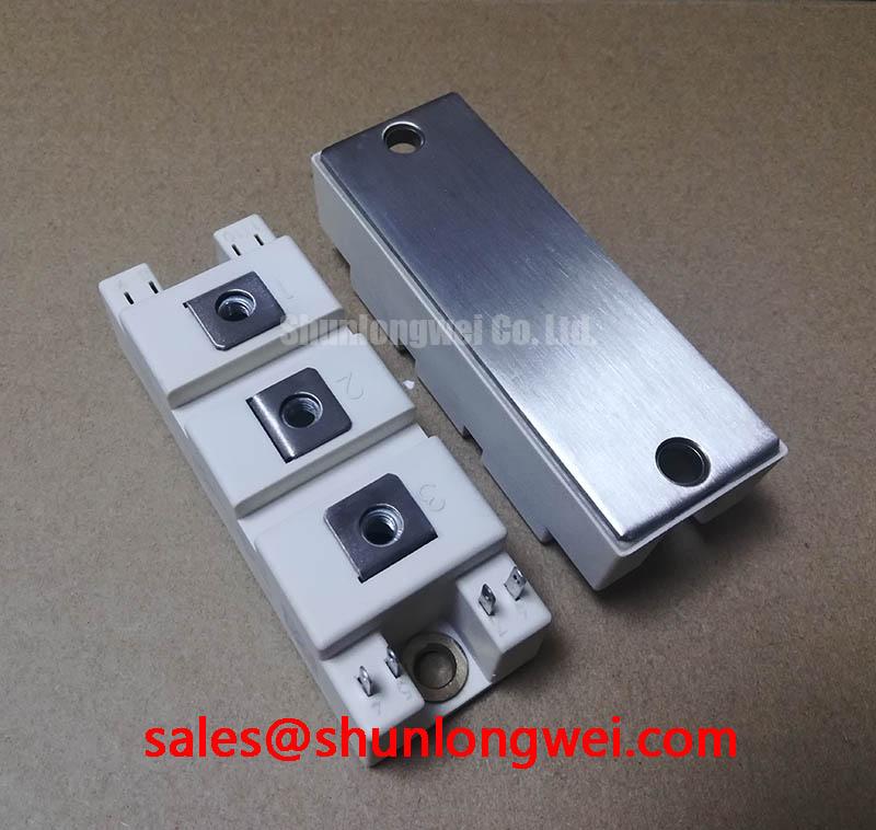
Where engineers are comparing physical and electrical interfaces across a repair platform, the BSM75GD120DLC can be reviewed as a separate IGBT module reference. It should not be treated as an automatic substitute for the FS75R12KE3_B9. The terminal structure, internal circuit arrangement, dynamic behavior, isolation arrangement, thermal interface, and required driver conditions must be verified from the relevant original documentation before any cross model installation.
⚠️ Field Alert: Isolate stored DC link energy and confirm a safe measured voltage before disconnecting module terminals or gate drive connectors.
FS75R12KE3_B9 Thermal Electrical Optimization: Turn Off di dt Induced V peak Clamping and Practical Tuning
Turn off behavior should be examined with voltage and current measurements taken at the module installation, because the circuit parasitics external to the FS75R12KE3_B9 influence the peak stress seen in service. In principle, peak voltage rises above the DC link level as stray loop inductance interacts with the rate of current change. The relationship is commonly expressed as DC link voltage plus stray inductance multiplied by current slew rate, but the measured result also depends on probe placement, switching state, clamp network behavior, gate drive timing, and the response of the surrounding capacitor network.
Engineering Recommendation: minimize the commutation loop inductance between the module and its local DC link capacitors to suppress turn off overshoot. A compact, symmetric planar busbar arrangement is often considered when equipment geometry permits, because it can reduce loop area and improve current path consistency. The actual layout must be validated with double pulse testing or representative switching measurements that verify peak voltage margin against the system DC link voltage and expected operating temperature.
Snubber or clamp circuitry, if used by the equipment design, must be treated as part of the original switching network. Its capacitor selection, resistor dissipation, placement, and connection length are system determined. An arbitrary change can reduce one visible voltage peak while increasing ringing energy, losses, or stress elsewhere. During troubleshooting, first inspect for displaced capacitors, cracked solder joints, changed busbar geometry, or connections that no longer match the original assembly. Then compare the turn on and turn off waveforms with the approved system baseline.
Thermal behavior requires equal attention. The module’s 75 A current rating is an official specification, but permissible continuous operating current in a finished converter depends on switching frequency, modulation method, cooling path, ambient temperature, load cycle, and protection settings. The mounting surface should be clean, flat, and free of debris that could create localized thermal resistance. Apply the interface material according to the equipment service procedure and maintain consistent clamping across the module mounting area.
For systems using parallel semiconductor positions, static current balance is influenced by the temperature dependent conduction characteristics of IGBT devices and by external conductor resistance. Positive temperature coefficient behavior can assist current sharing in certain operating regions, but it does not eliminate the need for matched busbar path length, symmetrical cooling, synchronized gate signals, and measured dynamic current balance. Design Consideration: do not assume that similar average current readings prove balanced turn off stress. Capture switching waveforms at the relevant operating states and assess each position under the same test conditions.
The Infineon IGBT paralleling application note provides useful technical context for engineers evaluating current sharing, layout symmetry, and dynamic matching. Its guidance should be read alongside the original converter documentation and the specific module data applicable to the installed assembly.
FS75R12KE3_B9 Operational Boundaries: Evaluating Common Mode Transient Immunity in Harsh I Limits
Common mode disturbances are often evaluated at the gate driver boundary rather than at the power module itself. The FS75R12KE3_B9 is rated at 1200 V and 75 A as official product specifications, but these figures do not define the common mode transient immunity of an installed driver board, digital isolator, optocoupler, auxiliary supply, current sensor, or control cable. The system integrator should verify the required isolation barrier, driver immunity, creepage distance, clearance distance, and measurement method from the original equipment documentation.
In a battery connected inverter or micro grid energy storage system, fast switching transitions can couple through parasitic capacitance into low voltage control domains. Potential symptoms include unexpected gate activity, irregular current measurement, controller resets, or communication errors. These observations do not establish a single root cause. Engineers should compare the gate to emitter waveform, driver supply stability, control ground reference, and switching node behavior while using measurement equipment suitable for high voltage power electronics.
Design Consideration: separate sensitive signal routes from high energy switching conductors wherever the mechanical design allows. Gate command and return paths should remain tightly associated, while control wiring should avoid long shared paths with switched power conductors. The effectiveness of this approach depends on the enclosure arrangement, cable routing, grounding strategy, driver isolation method, and actual switching waveform. Verification during representative load transitions remains essential.
A driver board with a specified reinforced isolation barrier or a stated common mode transient immunity rating should be assessed against the complete equipment voltage environment. Those values belong to the driver component specification, not to this IGBT module unless explicitly stated in its official documentation. Likewise, system compliance with electromagnetic compatibility requirements is determined by the completed equipment, including enclosure, filters, cable configuration, control hardware, and switching behavior. An individual IGBT module should not be represented as independently compliant with equipment level EMC standards.
When a power stage includes separate rectifier, front end, or complementary converter positions, the BSM75GB120DN2 may be relevant for reviewing the wider system topology. Any such review should distinguish its own ratings and interface requirements from those of the FS75R12KE3_B9. A shared current class or voltage class does not by itself establish electrical or mechanical interchangeability.
Protection coordination also deserves a direct check after service. Gate driver desaturation protection, soft turn off behavior, controller fault logic, current sensing, contactor operation, and semiconductor fuse coordination are interdependent layers. The equipment designer determines trip thresholds and response timing. For a suspected fault event, inspect the logged protection state where available, confirm the driver supply sequence, and verify that the fault shutdown path acts consistently before returning the system to energized testing.
Transient Dynamics & Electrical Design: High dv dt Cross Conduction Shoot Through on FS75R12KE3_B9
Cross conduction risk should be evaluated whenever complementary switches share a power leg. A rapid voltage transition at one device can capacitively influence the gate circuit of the opposing device. If the gate return path is inductive, the driver is unable to hold the intended off state, or timing overlap exists in the control sequence, an unintended conduction interval may occur. In a high energy DC link, this condition can demand more energy from the protection system than normal load switching.
Engineering Recommendation: use a gate driver architecture that actively maintains the commanded off state during switching node transients, subject to the driver and module documentation. Active Miller clamp functions, appropriately referenced gate returns, and gate drive arrangements with controlled off state behavior are common design approaches. The selected method must be verified in the installed converter because busbar geometry, gate loop routing, driver output impedance, temperature, and control timing all influence the result.
Negative gate bias is sometimes used in industrial switching systems as a Design Consideration to improve off state noise immunity. It is not an official operating requirement stated here for the FS75R12KE3_B9. The gate voltage range, driver supply rails, external resistance, clamp method, and switching timing must be taken from the applicable official module and driver documentation. System engineers should confirm the actual gate waveform directly at the relevant module terminals during switching tests, with particular attention to transient gate rise during the opposing switch transition.
Dead time should also be treated as a system controlled parameter, not a fixed rule that can be transferred between inverter platforms. Insufficient timing separation can contribute to overlap, while excessive separation may alter current commutation and distortion behavior. Verify the controller command signals, isolated driver outputs, and measured gate waveforms together. If behavior differs between operating modes, examine firmware mode changes, regenerative current direction, current controller saturation, and auxiliary supply stability rather than attributing the issue to one factor without measurement.
The Infineon IGBT modules and discretes portfolio provides manufacturer level context for IGBT power semiconductor technologies. For practical system review covering gate drive layout, thermal interfaces, and power stage topology, see IGBT Design & Integration. These resources support evaluation of the installed assembly, while the final suitability decision remains dependent on the original equipment circuit, protection architecture, and validated operating measurements.