
Content last revised on October 27, 2026
Transient Dynamics & Electrical Design: Planar Symmetrical Busbar Geometry for GD300HFY120C2S
I check the commutation path between the DC-link capacitor and module terminals before attributing a turn-off voltage spike to the GD300HFY120C2S itself. With the equipment isolated and stored energy discharged, tracing outgoing and return conductors reveals unnecessary loop area, offset connections and unsupported busbar sections. These external details affect switching behavior without changing the module’s 1200 V official voltage rating.
Design Consideration: the first-order engineering relationship Vpeak = VDC + Lσ × |di/dt| explains why collector-emitter voltage can rise above the DC-link voltage during current interruption. This simplified relationship excludes ringing and other circuit effects; its practical purpose is to identify which layout changes deserve measurement. Closely coupled planar conductors and balanced current paths can reduce commutation inductance, while conductor spacing must still satisfy the equipment’s insulation requirements.
Engineering Recommendation: favor a symmetrical busbar arrangement to reduce commutation-loop imbalance, then verify turn-off voltage margin with a suitably instrumented double-pulse test.
Snubber selection belongs to that measured circuit, not to a generic component recipe. Designers should assess oscillation frequency, damping, capacitor pulse capability and resistor dissipation together. Place the suppression network so its connections do not introduce a competing inductive loop. The discussion in Mastering Power System Dynamics provides supporting context for interpreting parasitic effects during switching tests.
Design Consideration: keep the gate-drive loop compact and its return path clear of power-current coupling. Evaluate Miller-induced gate excursions at the module connection rather than only at the driver output. Gate damping, any clamp function and driver-isolator common-mode transient immunity should be assessed against measured switching conditions, including probe limitations.
GD300HFY120C2S Operational Boundaries: Evaluating Dynamic Braking Chopper Operation Limits
Trace the braking branch on the equipment schematic before assigning braking duty to the GD300HFY120C2S. A module’s voltage and current ratings do not establish whether the installed circuit includes a braking switch, its associated resistor or the control needed to manage regenerated energy. Identify the actual switch connections and energy path before evaluating component suitability.
Design Consideration: a braking assessment should account for the energy returned during deceleration, the repetition pattern and the resistor’s pulse and average thermal loading. The switch must also remain within its applicable operating-area and thermal limits throughout the braking event. Designers should establish these requirements from the equipment’s load cycle rather than treating the 300 A official current rating as a permissible braking-current setting.
During commutation, diode reverse recovery interacts with circuit inductance and switching speed. Abrupt current recovery can excite ringing, but a noisy waveform alone does not identify the diode as the sole cause. Compare current and voltage waveforms with consistent probing, then assess snubber placement and gate-drive adjustments together. This is a Design Consideration for reducing switching disturbances, not an equipment-level EMC compliance claim.
Desaturation protection requires similar coordination. Its sensing behavior, blanking interval and fault turn-off profile must match the switch characteristics and application fault conditions. A controlled turn-off can limit inductive overshoot, but excessive delay also increases fault energy. Neither short-circuit withstand duration nor a protection threshold should be assigned to this model from its headline ratings.
For compatibility evaluation, engineers considering industrial inverter welders or medium-frequency induction-heating supplies should distinguish the inverter bridge from any separate braking or energy-management branch. The background references on power inverter topologies and pulse-width modulation and deadbeat control for current tracking explain system concepts; neither establishes this module’s switching limits.
Field Diagnostics & Commissioning: Main Terminal Pinout Mechanical Alignment in GD300HFY120C2S Topologies
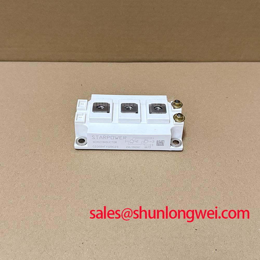
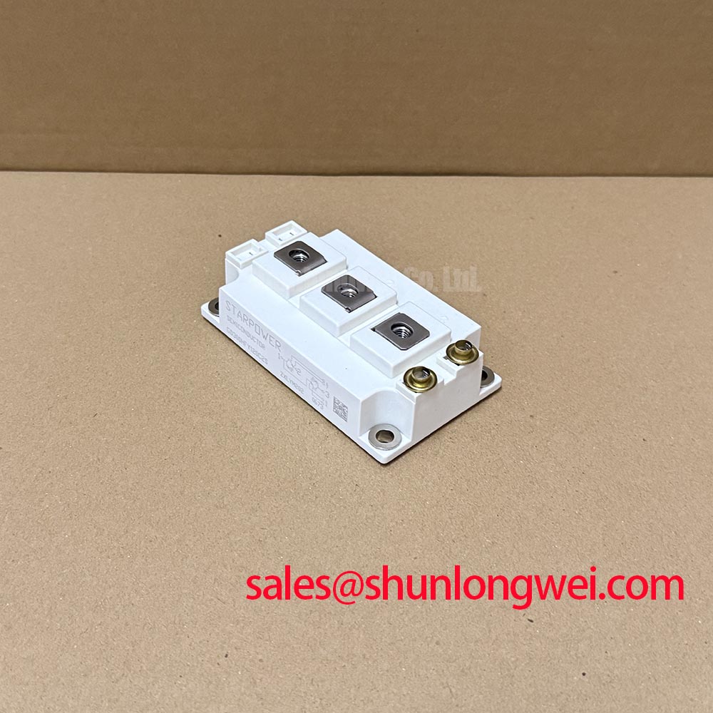
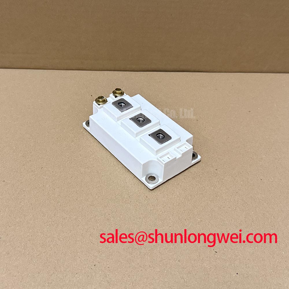
Align the busbar holes with the module terminals without using terminal screws to pull displaced conductors into position. Design Consideration: external busbars should have adequate support so that cable weight, assembly tolerances and thermal movement do not impose sustained bending loads on the terminal interface.
Match the terminal drawing to the equipment schematic before reconnecting the power stage. Identify power connections and gate-control connections from their documented functions, not from physical resemblance to another module. Where the original assembly uses a particular driver return arrangement, preserve that arrangement unless a validated circuit revision specifies otherwise.
Fastener engagement depends on the terminal construction, conductor stack and washer arrangement. Designers should check that the selected screw clamps the connection rather than bottoming out, and that washer seating remains flat. Apply the specified tightening procedure with a controlled tool; a generic screw-size torque is not a substitute for the module’s mounting instructions.
For sourcing comparisons, the related GD100HFU120C1S is a reference candidate for a specification comparison, not an established interchangeable replacement. Compare circuit configuration, rating conditions, terminal positions, mounting geometry and driver requirements individually. The shared manufacturer context does not resolve those differences.
Likewise, a component such as BSM300GA120DN2FS should be evaluated against its assigned schematic position when reviewing adjacent conversion stages. Its mention does not identify it as a rectifier or prove complementary operation. Record the actual device function and interface requirements before changing the assembly.
Transient Dynamics & Electrical Design: Optimizing Heatsink Contact Pressure on GD300HFY120C2S
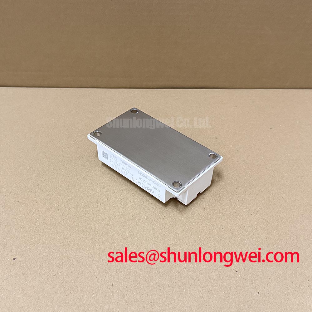
Inspect the heatsink contact surface for burrs, contamination and uneven support before placing the module. Design Consideration: thermal contact depends on surface condition, interface-material behavior and mounting pressure together. Increasing clamp force cannot reliably compensate for poor mating surfaces and can introduce unwanted mechanical stress.
Select the thermal interface material and application method for the documented mounting arrangement. Control coverage and trapped air without assuming that a universal grease thickness suits this package. Forcing the baseplate flat against an unsuitable surface is not a valid curvature-compensation method; assess mating-surface geometry within the applicable assembly requirements.
Use the prescribed tightening sequence to distribute contact pressure progressively, keeping terminal connections from disturbing the seated module. During commissioning, compare temperature behavior under repeatable load, coolant or airflow conditions. An unusual temperature rise can reflect interface contact, cooling performance or electrical loss, so inspect those contributors separately before attributing the result to the GD300HFY120C2S.